Download
1 / 36
360 likes | 490 Vues
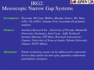
IRG2: Mesoscopic Narrow Gap Systems. Investigators: Doezema, McCann, Mullen, Murphy, Santos, Shi, Yang (OU); Xie (OSU); Salamo (UA); 6 postdocs/8 graduate students

E N D
IRG2: Mesoscopic Narrow Gap Systems Investigators: Doezema, McCann, Mullen, Murphy, Santos, Shi, Yang (OU); Xie (OSU); Salamo (UA); 6 postdocs/8 graduate students Partners:Amethyst Research Inc., University of Florida, Humboldt University (Germany), Intel Corp. , Ioffe Technical Institute (Russia), NTT Basic Research Laboratories (Japan), University of Texas at Austin, Tohoku University (Japan), SUNY Albany Motivation:Future technology needs can be addressed by nanoscale devices that exploit electron spin, quantum confinement, and ballistic transport.
Mesoscopic Device Examples gate source drain Gate Length~500nm Magnetic semiconductor Narrow-gap semiconductor Barrier metal Non-classical Classical • Magnetic Field Sensor • Working preliminary devices • Room-temperature operation • 30 nm width, diffusive transport • High electron mobility required • Spin Field-Effect Transistor • Studying spin injection and precession • Requires ballistic transport across interfaces and through channel
Goals of IRG-2 • Improved Narrow Gap Materials • Mesoscopic Magnetic Field Sensors • Fundamental Studies of Spin Effects in Semiconductors • Spin and Ballistic Transport Devices • Innovative Infrared Devices
C-SPIN Advantages • Leaders in InSb materials research: MBE, device processing, transport properties • Proficiency in optics: Self-induced transparency, coherent optics, ultra-fast pump-probe • Inventor of Interband Cascade Laser for infrared applications Mars Science Laboratory (MSL)
MBE GROWTH • InGaAs/AlInAs • InAs/AlSb/GaSb • InSb/AlInSb • THEORY • Screened Atomic Pseudopotentials • Spin Transport • OPTICS • Spin Lifetimes • Spin-Orbit Effects • Infrared Devices • CHARACTERIZATION • STM, AFM • TEM, SEM • X-ray Diffraction • FTIR • Hall Effect • TRANSPORT • Quantum Confined Devices • Ballistic Transport Devices • EMR and m-Hall Devices • FABRICATION • Photolithography • E-beam Lithography • Reactive Ion Etching • Surface Gates Mesoscopic Narrow Gap Systems
MBE GROWTH • Santos • Salamo • ARI collaborators • THEORY • Mullen • Xie • Ioffe collaborator • Florida collaborator • OPTICS • Yang • Salamo (Guzun) • McCann • Shi • Doezema • CHARACTERIZATION • Santos (Mishima) • Salamo • Murphy • Doezema • TRANSPORT • Murphy • Salamo (Kunets) • NTT/Tohoku collaborators • FABRICATION • Murphy • NTT/Tohoku collaborators • Humboldt collaborators • Intel collaborators Mesoscopic Narrow Gap Systems
Strategy/Progress IRG2 Transport Optics Growth Theory InSb APL 91, 062106 (2007) Phys Stat Sol, 2775 (2008) JCG 311, 1972 (2009) Theory PRL 101, 046804 (2008) PRB 77, 035327 (2008) PRB 78, 045302 (2008) Spin Lifetime Spin Transport Physica E 34, 647 (2006) Springer 119, 35 (2008) Interband Cascade Lasers Elec Lett 45, 48 (2009) InGaAs APL 91, 113515 (2007) APL 92, 222904 (2008) APL 94, 013511 (2009 Magneto-optics APL 89, 021907 (2006) JVST B24, 2429 (2006) Springer 119, 213 (2008) Hall Sensors J Mat Sci 19, 776 (2008) IEEE TED 56, 683 (2009) Infrared Devices JAP 101, 114510 (2007) IEEE PTL 20, 629, (2008) APL 92, 211110 (2008) IV-VI APL 88, 171111 (2006) Physica E 39, 120 (2007)
Mesoscopic Narrow Gap Systems • Molecular Beam Epitaxy of narrow gap materials • Spin related experiments and associated theory • Spin-relaxation optical measurements • Spin-orbit transport experiments • Theory and modeling of spin-orbit devices • Narrow-gap electronic devices • InGaAs-based electronic device structures • High-mobility hole systems • Narrow-gap photonic devices • III-V Interband Cascade (IC) Lasers • IV-VI infrared and thermoelectric applications
IV-VI Semiconductors • Band gap in mid-infrared • High thermal conductivity
Electron Mobility and Structural Defects in n-type InSb QWs 4×10⁴ Santos (111) glide plane Mobility @RT (cm2/Vs) 54.7° 3×10⁴ 2×10⁴ 0 1.8×10⁹ 0 6×10³ TD density (/cm2) 3.6×10⁹ 31° 1.2×10⁴ MT density (/cm) Misfit dislocations 1μm 220 Dark-field (DF) X-TEM Record high mobility for a QW at room temperature when structural defects are minimized. APL 91, 062106 (2007).
Mesoscopic Narrow Gap Systems • Molecular Beam Epitaxy of narrow gap materials • Spin related experiments and associated theory • Spin-relaxation optical measurements • Spin-orbit transport experiments • Theory and modeling of spin-orbit devices • Narrow-gap electronic devices • InGaAs-based electronic device structures • High-mobility hole systems • Narrow-gap photonic devices • III-V Interband Cascade (IC) Lasers • IV-VI infrared and thermoelectric applications
Spin Orbit Effects Bulk Inversion Asymmetry Structural Inversion Asymmetry Rashba splitting Dresselhaus splitting • Large effects predicted in narrow gap materials • Spin splitting at zero magnetic field • Spin precession • Spin-dependent ballistic trajectories
Spin Related Experiments and Theory Salamo (UA) Murphy, Santos, Mullen (OU) Xie (OSU) Golub (Russia) NTT Basic Research Laboratories (Japan) Tohoku University (Japan) Optical Spin Measurements Spin Transport NMR Studies Theory
Optical Measurements of Spin Relaxation Salamo, Murphy, Santos Mechanisms Elliot-Yafet (spin orbit) Dyakanov-Perel (inversion asymmetry) Bir-Aranov-Pikus (spin exchange with holes) Hyperfine interactions State of the Field GaAs extensively studied InAs studied InSb limited studies
Optical Measurements of Spin Relaxation Salamo, Murphy, Santos
Optical Measurements of Spin Relaxation Salamo, Murphy, Santos Bulk InSb Elliot-Yafet mechanism responsible for spin relaxation in bulk InSb Future work: Quantum Wells Confinement Energy, Confinement Asymmetry
Spin Transport Measurements Murphy, Santos First observation of current focusing peaks in InSb heterostructures. Physica E 34, 647 (2006).
Spin Transport Measurements BT B║ B┴ θ Murphy, Santos Doublet is related to spin. • Current Effort and Future Work: • Improved Gating with NanoTech UCSB & Penn State NanoFab • Spin Interferometers (Rings and Ring Arrays) Physica E 34, 647 (2006).
Weak Anti-Localization Measurements Murphy, Santos, Golub Good agreement with theoretical predicted values of spin-orbit coupling in InSb. Future: study WAL as a function of gate voltage and applied strain. Springer Proc. Phys. 119, 35 (2008).
Designing Spin-Orbit Coupling Mullen, Murphy, Santos ASYMMETRIC SYMMETRIC Future Work: Design structure to maximize change in S-O with applied gate voltage.
Spin and Spin Hall Theory Xie • Proposed Device • Non-uniform Rashba effect • Spin interference • Current predicted to be ~10% spin polarized • Device not yet realized Spin Nernst Effect Persistent Spin Currents PRB 77, 035327 (2008) PRB 78, 045302 (2008)
Mesoscopic Narrow Gap Systems • Molecular Beam Epitaxy of narrow gap materials • Spin related experiments and associated theory • Spin-relaxation optical measurements • Spin-orbit transport experiments • Theory and modeling of spin-orbit devices • Narrow-gap electronic devices • InGaAs-based electronic device structures • High-mobility hole systems • Narrow-gap photonic devices • III-V Interband Cascade (IC) Lasers • IV-VI infrared and thermoelectric applications
Gated Narrow-Gap InxGa1-xAs QWs Epilayers for high-k integration (UT Austin, Jack Lee) HfO2 Epilayers for high-k integration (Penn State/Cornell, Darrell Schlom) LaAlO3 Epilayers for high-k integration (SUNY Albany, Serge Oktyabrsky) ZrO2 • Challenges for III-V transistors • Stable & reliable gate dielectric • Integration with Si substrates • p-channel III-V FET for CMOS MBE growth (C-SPIN, Santos) InxGa1-xAs/InxAl1-xAs MBE Epilayer characterization (C-SPIN, Santos) HRXRD, Hall effect, AFM, TEM Scanning Tunneling Microscopy/Spectroscopy (UC San Diego, Andrew Kummel) Ga2O, and In2O 8 journal articles since 2007 on ZrO2, HfO2, LaAlO3 on InxGa1-xAs
Effective Mass of Holes in InSb QW Doezema, Santos, Stanton p-FET n-FET • Low-T mobility (~50,000 cm2/Vs) consistent with effective mass • 300K mobility (700 cm2/Vs) much lower than expected Cyclotron Resonance at 4.2K APS 2009
p-type InSb Quantum Well Al0.10In0.90Sb 30 nm Be d-doping Al0.10In0.90Sb Al0.20In0.80Sb 20 nm Al0.20In0.80Sb 15nm InSb well Al0.20In0.80Sb Buffer Layer GaAs (001) substrate Santos Be d-doping • First realization of remotely-doped p-type InSb QWs.
Integration of InSbn-FET and Gep-FET Santos Ge Ge InSb InSb p-FET p-FET n-FET n-FET GeOI BOX = Buried Oxide Ge substrate Si substrate Ge substrate type GeOI / Si substrate type Amethyst Research Inc. p-type n-type APS 2009
Mesoscopic Narrow Gap Systems • Molecular Beam Epitaxy of narrow gap materials • Spin related experiments and associated theory • Spin-relaxation optical measurements • Spin-orbit transport experiments • Theory and modeling of spin-orbit devices • Narrow-gap electronic devices • InGaAs-based electronic device structures • High-mobility hole systems • Narrow-gap photonic devices • III-V Interband Cascade (IC) Lasers • IV-VI infrared and thermoelectric applications
Interband Cascade (IC) Laser InAs/Al(In)Sb multilayers AlSb InAs hv GaInSb AlSb GaSb AlSb InAs/Al(In)Sb multilayers hv Yang, Johnson, Santos E many photons per electron e hv type-II broken gap alignment hv hv hv Cascading • cascade process — • high efficiency, large output power, uniform injection over every stage, low carrier concentration, thus lower loss • interband transition — • circumvents fast phonon scattering hv hv hv • quantum engineering at sub-nanometer scale and Sb-based type-II QW system • suppresses non-radiative Auger losses • allows for wide wavelength tailoring range • excellent carrier confinement because of band-gap blocking feature Low threshold current, high efficiency, high output power mid-IR lasers
Preliminary Results of Interband Cascade Lasers A broad-area (150mm x 1.9mm) device lased in continuous wave (cw) mode up to 150 K near 6 mm, the longest attained, to date, for III-V interband diode lasers. Electron. Lett. 45, 48 (2009)
Latest Results 11-stage IC laser Jth~82 A/cm2, Vth~2.3V, at 84K • Lower threshold current density and operating voltage • Lasing wavelength ~7.4 mm • Longer wavelengths possible
Where are we? J - JPL N-NRL III-V Sb-based mid-IR diode lasers reported in literature and OU- University of Oklahoma Device fabrication and package are in a preliminary stage for ICLs Our latest lasers operate up to 121 K near 7.4 mm, now the longest attained to date, for III-V interband cascade lasers.
PbSe Quantum Wires for Thermoelectric Applications [110] [110] [110] 200 nm 200 nm 200 nm 2 ML PbSe CaF2 CaF2 PbSe QWR McCannRidge-groove CaF2 structure and subsequent PbSe growth. AFM of 2 ML PbSe Grayscale: 95 nm • CaF2 growth on Si (110) adopts a ridge-groove morphology • Subsequent growth of PbSe produces quasi-one-dimensional structures indicated by a 200 meV blue shift in PL • Improved thermoelectric properties predicted, based on enhanced electrical conductivity, but reduced thermal conductivity, along wires. • TE figure of merit, ZT σ/κ, σand κ, electrical and thermal conductivities, resp.
PbSe Micro/ Nanostructures PbSe bulk 4 μm 4 μm Shi Strain in MQW causes rolling of PbSe when BaF2 layer is removed in water. PbSe layers BaF 2 layer PbSe bulk SEM image and PL of a freestanding MQW microtube. Diameter 600, length 5 mm. SEM images and PL of PbSe micro-rods. APL88, 171111 (2006). Physica E39, 120 (2007).
IRG2: Mesoscopic Narrow Gap Systems • Comprehensive expertise: MBE, characterization, fabrication, transport and optical experiments, theory • Fundamental and technologically motivated studies • Devices exploit high mobility, quantum confinement, ballistic and spin effects
Strategy/Progress IRG2 Transport Optics Growth Theory InSb APL 91, 062106 (2007) Phys Stat Sol, 2775 (2008) JCG 311, 1972 (2009) Theory PRL 101, 046804 (2008) PRB 77, 035327 (2008) PRB 78, 045302 (2008) Spin Lifetime Spin Transport Physica E 34, 647 (2006) Springer 119, 35 (2008) Interband Cascade Lasers Elec Lett 45, 48 (2009) InGaAs APL 91, 113515 (2007) APL 92, 222904 (2008) APL 94, 013511 (2009 Magneto-optics APL 89, 021907 (2006) JVST B24, 2429 (2006) Springer 119, 213 (2008) Hall Sensors J Mat Sci 19, 776 (2008) IEEE TED 56, 683 (2009) Infrared Devices JAP 101, 114510 (2007) IEEE PTL 20, 629, (2008) APL 92, 211110 (2008) IV-VI APL 88, 171111 (2006) Physica E 39, 120 (2007)