Download

1 / 18
190 likes | 920 Vues
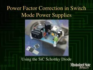
Power Factor Correction in Switch Mode Power Supplies. Using the SiC Schottky Diode. Team. Team Leader Robin Kelley Team Members Travis Brignac Clinton Livingston. Abstract.

E N D
Power Factor Correction in Switch Mode Power Supplies Using the SiC Schottky Diode
Team • Team Leader • Robin Kelley • Team Members • Travis Brignac • Clinton Livingston
Abstract • Design a switch mode power supply with a new power factor correction circuit, which implements the SiC Schottky diode. • Issue Application Note detailing use of the SiC Schottky diode in power factor correction
Motivation • Current power supply technology, uses Si pn junction diodes. • These Si pn junction diodes create reverse recovery current problems within the power factor correction (PFC) circuitry • SiC Schottky diode will eliminate reverse recovery current in PFC circuitry
Comparison: Si pn vs. SiC Schottky • Reverse biased pn junction diode does not turn off fast enough during switching • This is due to the removal of excess carries from the depletion region • Causes reverse recovery transient
Comparison (cont.) • SiC Schottky diodes do not need to remove excess carries from the depletion region • Eliminates reverse recovery transient.
Implementation • Switch mode power supply industry is extremely vast • Need one specific application for implementation of new PFC circuitry • Electronic Ballast will be used for implementation
System / Hardware 120V AC
Design Constraints • Power Factor Correction circuit operation of 100kHz • Smaller passive components • More efficient circuitry • Operation in Continuous conduction mode • Reduced EMI problems • EMI Filter operational at 100kHz • DC-AC Inverter operation at 100kHz • As frequency increases lamp efficiency increases
Design Constraints • Ballast must operate below IEC 1000-3-2 Class C harmonic limitations of 30% • Meet power loss and efficiency factor of 87% seen in current ballast design • Product will operate according to North American 120V/60Hz operation
Design Constraints • Operating Temperature range of –20º to 50 º C • Product will not exceed standard electronic ballast measurements of 8.3” x 2.22” x 1.6” • Develop application note for use of the SiC Schottky diode
Testing Specifications • Software • P-Spice - used to layout original circuit design and run initial simulations • Orcad Layout Plus – used to layout board design for circuitry • Hardware • O-scope – used to plot waveforms of voltages and currents to determine correct operation of each stage of circuitry, detect noise and transients. • Digital Multi-meter- used to measure and insure correct voltage and current levels • Thermo-couple- used to measure operating temperature of circuitry
Current / Future Work • Finalizing component sizing and selection • Working on circuitry design • P-Spice Simulations to complete design
Project Deliverables • Electronic ballast with operational PFC circuitry using the SiC Schottky diode, redesigned EMI filter, and Inverter based on an operating frequency of 100kHz. • Applications Note detailing the entire design process of the project and promoting the use of the SiC Schottky diode in power factor correction.
Acknowledgments • Thank You to Dr. Michael S. Mazzola, our advisor, for his guidance and input. • Thanks to Jim Gafford, Dr. Joseph Picone, Bill Buchanan and Wey Beng for their support
References • [1] H. Kapels, I. Zverev, R. Rupp, and L. Lorenz, “SiC Schottky diodes: A Milestone in hard switching applications,” Application Note, Infineon Technologies, 2001. • [2] Marco Scherf and Ilia Zverev, “200W SMPS Demonstration Board,” Application Note, Infineon Technology, v1.2, November 2001. • [3] M. Bairanzade, “Electronic Lamp Ballast Design,” Application Note, Motorola, 1995. • [4] “SWITCHMODEPower Supplies Reference Manual and Design Guide,” Manual, ON Semiconductor, Rev.3, July 2002. • [5] “Infineon Technologies Produces World’s first Power Semiconductors in Silicon Carbide,” http://www.infineon.com/news/press/102-019e.htm, Infineon Technologies AG, Muenchen,Germany, February 5, 2001 • [6] C. Miesner, R. Rupp, H. Kapels, M. Krach, and I. Zverev, “thinQ!™ Silicon Carbide Schottky Diodes: An SMPS Circuit Designer’s Dream Comes True!,” Technical White Paper, Infineon Technology, Infineon Technologies AG, September, 2001. • [7] Ming Hian Chew, “Design of Power Factor Correction Circuit Using GreenlineE Compact Power Factor Controller MC33260,” Application Note for AND8016/D, ON Semiconductor, June 2002. • [8] Product Information E2/32IS-120 Two Lamp Operation, 120V, Howard Industries, Inc., February 2001.