Outcome 1 - Contents
1.98k likes | 2.27k Vues
Outcome 1 - Contents. 1 Data Representation 2 Computer Structure 3 Computer Performance 4 Peripherals 5 Networking 6 Using Networks 7 Computer Software 8 Supporting Software. 1 Data Representation 1.1 Introduction. Lowest level in computer only binary numbers can be used.

Outcome 1 - Contents
E N D
Presentation Transcript
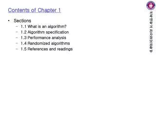
Outcome 1 - Contents • 1 Data Representation • 2 Computer Structure • 3 Computer Performance • 4 Peripherals • 5 Networking • 6 Using Networks • 7 Computer Software • 8 Supporting Software
1 Data Representation 1.1 Introduction • Lowest level in computer only binary numbers can be used. • We work in base 10. • Computer must be able to process +ive and –ive, very large and very small numbers. • We look at how the computer uses numbers to represent text and graphics
1 Data Representation 1.2.1 Decimal Numbers • We use base 10 • When expressing large numbers in terms of powers of 10 the following abbreviations are used: • 101 = 10 • 102 = 100 • 103 = 1000 = 1 kilo • 106 = 1,000,000 = 1 Mega • 109 = 1,000,000,000 = 1 Giga • 1012 = 1,000,000,000,000 = 1 Tera
1 Data Representation 1.2.1 BinaryNumbers Computers work in number base 2 which uses 2 symbols, 0 and 1 to represent a value. In computing systems, large numbers are expressed in terms of powers of 2 and use the following abbreviations: 21 has a decimal equivalent of 2 22 has a decimal equivalent of 4 23 has a decimal equivalent of 8 24 has a decimal equivalent of 16 25 has a decimal equivalent of 32 26 has a decimal equivalent of 64 27 has a decimal equivalent of 128 28 has a decimal equivalent of 256 29 has a decimal equivalent of 512 210 has a decimal equivalent of 1024 and is abbreviated to 1 kilo 220 has a decimal equivalent of 1,048,576 and is abbreviated to 1 Mega 230 has a decimal equivalent of 1,073,741,824 and is abbreviated to 1 Giga 240 has a decimal equivalent of 1,099,511,627,776 and is abbreviated to 1 Tera
1 Data Representation1.2.2 Decimal to Binary • How to convert decimal to binary e.g. 29 Giving 11101 • Using 1 byte for storage gives 256 possible numbers. • 2 byte gives 65536, 0-65535 • Increasing the size of the storage for numeric data increases the range of numbers which can be stored.
1 Data Representation1.2.3 Binary to Decimal • Numbers converted to binary – number base 2 • Example of 154 represented as a binary number =154
1 Data Representation1.2.4 Hexadecimal Long binary numbers can be difficult to read correctly. Computers have memory addresses of 2 or 4 bytes long which give addresses of 16 or 32 bits. Hexadecimal is base 16 and organises the bits into groups of four. The conversion between base 2 and base 16 is very simple. Hex needs the digits 0-9 and letters A-F. E.g. 11010100010110010011001010010110 becomes 1101 0100 0101 1001 0011 0010 1001 0110 which in Hex is D459 3256
1 Data Representation1.2.5 Why Binary • Logic circuits based on two state logic – use only 0 and 1. • We only need two voltages 0 and a voltage of any value = 1 • There are only 4 rules of arithmetic with binary (100 in base 10). • Robust – can cope with degradation of signal.
Data Representation1.2.6 & 1.2.7 Integers • Positive numbers • Converted directly to binary • 2 bytes = 16 bits gives 0 to 216-1 or 0 to 65535 • n bytes gives n*8 bits - 2n*8 - 1 • Negative Numbers • 216 : Same range but –32768 to 32767 • Using sign bit 0 +ive and 1 –ive e.g. 011 = 3 and 111 = -3 • Sign and magnitude does not work because: • Addition does not work properly (-5+-10 gives 15) • Two 0’s (00000000 and 10000000)
Data Representation1.2.8 Twos Complement • Two’s Complement is another way of representing negative numbers. • Addition works and there is only one zero • All 0’s are converted to 1’s and 1’s to 0’s then 1 is added. • To convert 5 to –5 OR 5 OR -5
Data Representation1.2.9 Real Numbers • Real numbers are stored as floating point or scientific notation. Numbers stored as base and exponent. • E.g 34008.6 is .340086*105 • In binary 1101.1001 is .11011001*2100 (the 4is 100 in binary) • The mantissa is 11011001 and the exponent is 100 • Usually 4 bytes used for mantissa and 2 for exponent • Increasing the size of the mantissa increases accuracy • Increasing the size of the exponent increases the range of numbers which can be stored
1 Data Representation1.3 Text ASCII • Each character is stored in an 8 bit binary code called the ASCII system. • E.g. A is stored as 65 (01000001 in Binary). • 1 byte can store 256 different characters – enough for all the keys on the keyboard and several foreign symbols (for currency etc.). • Unicode • Need to represent non-Latin chars e.g. Japanese and Chinese • Characters encoded using 16 bits – 65,536 symbols. • MS Office stores documents in Unicode
Data Representation1.4 Graphics Most displays use Raster graphics – same as TV. Displays store images as a matrix of pixels in the refresh buffer. Separate images now stored in VRAM (Video RAM). VRAM represents the entire screen area and the term bit map is used to describe the one-to-one mapping of pixels in VRAM to pixels on the screen.
Data Representation1.4.1 Bit-mapped Graphics • For a graphic drawn in a painting package the computer stores the data as a 2 dimensional array of pixels. • Each pixel in a black and white image is 1 bit in memory. • 2 bits can store 4 colours or shades of grey. • 8 bits can store 256 colours. • The number of bits used for each pixel is the bit depth. • The resolution is the number of pixels in the height and width of the image. • Bit mapped images are often generated from scanned pictures and can create huge files. • Editing can be performed at pixel level. • When images are enlarged they can become “lumpy” and lose definition.
Data Representation1.4.2 Calculating Memory Requirements • We need to know the size of the image, resolution and bit depth. • Size – usually inches e.g. 6” x 4” • Resolution – say 500 dpi (pixels per inch) • Bit Depth – e.g. 1 bytes for 256 colours No of bytes is
There are many different ways of arranging the bytes that hold image information, but one way is to map them so that the first byte represents the top left pixels, the second byte represents the pixels to the right of the first pixel, until the end of the first row is reached, when the next byte holds the information for the left hand end of the second row. For a small (24 pixel by 4 rows ) display the layout would look like this: Data Representation1.4.3 Arranging The Bytes The image is saved as a series of bytes to a storage device, such as memory or disk.If we wish to review the image then it is a simple matter to transfer the image data back into the video memory as a direct copy. As this image is also in a bit mapped format, we can still move it to and from other storage devices without any translation.
Data Representation1.4.4 Greyscale A rudimentary greyscale effect provides a ’black’, ’white’ and two levels of ’grey’. As this comprises four different values we need two bits to represent each pixel (00 for black, 01 for darker grey, 10 for lighter grey and 11 for white ). As each pixel now requires twice as many bits, we will require twice as much memory for a given screen size as a black and white image. We can provide more levels of grey by allocating more bits to each pixel. By the time we have eight bits (one byte) to one pixel we can represent 256 different intensities. Monochrome displays are often clearer, especially for text than colour display. The requirement to use colour for such items as colour pictures and user interface issues, dictates that colour displays are more likely to be purchased.
Data Representation1.4.6 Compression • A colour bit – mapped image with a high resolution and 24 bit colour needs a lot of storage (50MB for a smallish photo). • File compression is used to reduce storage requirements. • Different techniques – coding using and index of colours actually used and not coding differences indistinguishable to the human eye.
Data Representation1.4.5 Colour One colour can be represented by one byte giving 256 colours (GIF format). Monitors etc. have 3 primary (additive) colours, Red, Blue and Green. Other colours obtained from adding light. We use 8 bits for Red, 8 for Blue and 8 for Green which give us 256 x 256 x256 colours – over 16 million. We need 3 bytes to describe RGB coded colours. Codes can be used by a programmer to describe colours in Hex code.
Data Representation1.4.7 Vector Graphics • Objects not described pixel by pixel but by its attributes (start & end positions, thickness & colour of lines etc.) • Sometimes called object-orientated graphics. • Vector graphics are resolution independent. Rasterisation need for conversion to bit map for display or printing. • Editing at pixel level not possible. • Can be scaled without losing original image quality • Less storage required • Can be grouped and edited at the object level. • Can be placed over another graphic without rubbing it out as happens with bit-mapped.
2 Computer Structure2.1 An Introduction This unit on Computer Structure describes in detail the function of the component parts of a processor in the manipulation of data. This is extended to the methods of transferring data within a processor and between a processor and memory. The concept of a stored program is considered and the steps in the fetch-execute cycle to access and run programs. Memory types are considered, from registers to backing storage and how memory is defined and addressed.
2 Computer Structure2.2 Computer Organisation • Computers play a significant role in meeting our everyday requirements. You can now browse the Internet for: • a new home, • Shop on-line and have home delivery • import a new car from abroad • order clothes from a catalogue company • communicate with friends overseas. • The ways in which you learn are also changing. • On-line homework • Computer based learning tools
2 Computer Structure2.2 Computer Organisation • It makes sense to find out how they work and how you can make use of them. • How are they structured? • How do they operate? • How is data represented? • Why are some computers more powerful than others? • What devices can you attach? • How do they communicate? • Answers can be found in the following Topic
2 Computer Structure2.2. Calculating Machines- From Babbage to VLSI • Abacus developed about 1300 AD by Chinese • Logarithms developed by John Napier • Other manual devices developed by Pascal & Liebniz • First mechanical calculator developed by Charles Babbage (1792 – 1871) Difference Engine and then Analytical Engine. • Idea of stored program concept developed. • First Electrical machine Enigma codebreaker in WW2. • Vacuum tubes (40’s replaced by transistors (60’s) • From 1965 to present circuitry all on one chip Integrated circuits. • Now we have VLSI (Very large Scale Integration)
2 Computer Structure2.2.1 A Two State Machine • Typical 4 box diagram • Only 2 states used in all components and data storage, on or off, 1 or 0. • Advantages of 2 state. • Simplicity – 2 voltage levels. • Good tolerance • Simple calculations. CPU Processor Input Output Memory RAM & ROM Backing Storage
2 Computer Structure 2.2.2.1 The structure of the CPU (a) Memory Processor Control unit Control Bus Internal buses ALU Data bus – 2 way Registers, A, MAR, MDR, PC, SP Address bus – 1 way
2 Computer Structure 2.2.2.1 The structure of the CPU (b) • ALU (Arithmetic & Logic Unit) • Data is processed and manipulated. • Involves arithmetic operations and logical comparisons. • Control Unit • Manages execution of instructions. • Sends control signals around the computer. • Registers • Storage location with the CPU • Hold calculations, store addresses etc. • Main Memory • External Memory • Peripheral Devices
2 Computer Structure 2.2.3 The stored program concept All computers based on same basic design, known as the Von Neumann Architecture. Computers carry out tasks by executing machine instructions. A series of these instructions is called a machine code program held in main memory as a stored program, a concept first proposed by John Von Neumann in 1945. Central Processing Unit (CPU) fetches, decodes and executes the machine instructions. By altering the stored program it is possible to have the computer carry out a different task.
2 Computer Structure 2.2.4 The fetch execute cycle To execute a machine code program it must first be loaded, together with any data that it needs, into main memory (RAM). Once loaded, it is accessible to the CPU which fetches one instruction at a time, decodes and executes it at electronic speed. Fetch, decode and execute are repeated until a program instruction to HALT is encountered. This is known as the fetch-execute cycle.
2 Computer Structure 2.2.4.1 The fetch execute cycle in detail • This is how the: • Address bus • Data bus • Control Bus • Registers • All take part in reading an instruction from memory and executing it.
2 Computer Structure 2.2.4.3 The fetch phase . 1. The contents of the PC are copied into the MAR; 2. The contents of memory at the location designated by the MAR are copied into the MDR; 3. The PC is incremented; 4. The contents of the MDR are copied into the IR. 2.2.4.4 The Execute phase 1. Decode the instruction in the IR; 2. Execute the instruction in the IR.
2 Computer Structure 2.2.8 Computer Components and Their Function The components of the CPU and the connections to devices that are external to it are shown.
2 Computer Structure 2.3 Memory Main memory (RAM and ROM) stores programs and data while the computer is operating. • Any location in memory can be read from or written to by referring to its address. • Memory can be organised as: • 8- bit wide (PC-8088) • 16-bit wide (XT-8086, AT-80286) • 32-bit wide (386DX, 486SX, 486DX) • 64-bit wide (Pentium)
2 Computer Structure 2.3.1 RAM • RAM • Has same access time for all locations. • Volatile – loses contents on power off. • 2 Types of RAM Static and Dynamic • Static – holds contents as long as there is power. • Dynamic – has to be refreshed (every 2 ms). • Each memory location has a unique address.
2 Computer Structure 2.3.2 ROM • ROM • Contents permanent or non-volatile. • Software & data fixed into ROM at manufacture. • Operating systems and specialised ROMs (e.g. cameras and CD players etc.). • Some ROMs can be reprogrammed • EPROM – electrically programmable read only memory (data erased by ultraviolet light and new program burned onto ROM • EEPROM – electrically erasable programmable read only memory – selective parts can be reprogrammed & used in developmental work
2 Computer Structure 2.3.4 Cache Memory • Faster processors mean data is being processed before the next instructions can be read from memory (system busses slow). • Most systems have 2nd smaller area of fast SRAM. Next instructions read into cache – much faster than RAM.
2 Computer Structure 2.3.6 External Memory • External memory, such as the hard disk, holds quantities of data too large to store in main memory. • It is also used to keep a permanent copy of programs and data. • Examples of external memory devices are: • hard disk; • floppy disk; • zip disk; • CD-R; • magnetic tape; • flash drive.
2 Computer Structure 2.4 Central Processing Unit Central Processing Unit. The CPU coordinates and controls the activities of all other units in the computer system. It executes program instructions and manipulates data in accordance with the instructions. It uses a standard architecture composed of the following three components: Arithmetic and logic unit (ALU); Control unit; Registers. All three components work together to form the processor.
2 Computer Structure 2.4.1 Architecture of the microprocessor We will now study the internal architecture of the microprocessor (CPU) itself. Because of the stored program concept, we must consider the relationship between the CPU and memory. This is a diagram of a fairly typical microprocessor design, showing the internal structure of the CPU and its relationship to the memory of the computer.
2 Computer Structure 2.4.2 Accessing Memory The CPU has to access memory both for instructions and to receive and transmit data from or to memory. Memory Address Register (MAR) - specifies the address in memory for the next read or write operation from or to memory; The Memory Data Register (MDR) or Memory Buffer Register (MBR) - contains the data to be written to memory or receives the data read from memory. • MAR register connected to the address bus • MDR register connected to the data bus.
2 Computer Structure 2.4.2 Accessing Memory (2) The MAR and MDR registers have a large part to play in the fetch-execute cycle. To read data from memory, CPU places the address of the memory location into the MAR and activates the memory-read control line of the system bus. This will cause the required data to be transmitted from memory via the data bus to the MDR; To write from the CPU to memory, the CPU places the data to be written in theMDR; the address of the memory location where they are to be written is placed in the MAR; and the memory-write control line is activated.
2 Computer Structure 2.4.3 Functions of Control Bus • Control bus has several lines, used singly to initiate a process. • Read Line – initiates memory read operation. • Write Line - initiates memory write operation. • Clock – Generates pulse to synchronise components. • Interrupt – Signal to processor of an interrupt like a key press or mouse click. Processor saves stack and deals with the interrupt. • NMI – Non-Maskable Interrupt. Interrupt which cannot be ignored. • Reset – Clears all registers, aborts program and gives control back to the operating system.
2 Computer Structure 2.4.3.1 Getting the processors attention • Polling • The processor checks each part of the system in turn and if any part wants the processors attention it signals to the processor. • Interrupts • This is how a PC works. When a key is pressed or mouse clicked an interrupt is generated and the processor carries out that task (sometimes it is “doing nothing” and is interrupted. • Some interrupts need not be actioned (Maskable Interrupts), others must be actioned (NMI) e.g Ctrl+Alt+Del
2 Computer Structure 2.4.4 The Arithmetic Logic Unit • ALU • Where data is processed and manipulated. • ALU involves arithmetic operations and logical operations . • ALU uses temporary registers to hold data. • Accumulator is main register.
2 Computer Structure 2.4.5 Registers • memory address register (MAR) holds address of a location in main memory. • memory buffer register (MBR) holds data that has just been read from main memory or is to be written to main memory. • instruction register (IR) holds the current instruction that is being executed. • program counter (PC) holds the address of the next instruction to be fetched from memory. • Processor also has a set of general purpose registers. They are called general purpose because their role is not defined at manufacture and can be used by programmers as appropriate.
Data is transferred between memory and processor by buses. Address Bus Pinpoint memory location. One-way Bus Data Bus Transfers the data Same size as Word size Two-way Bus Control Bus Initiates and controls operations. Inside the processor. 2 Computer Structure 2.5 Buses Control Unit Control Bus Memory Data Bus Processor Address Bus
2 Computer Structure 2.5.1 Addressability • The Word Length is the size of data, in bits, which can be manipulated as a single unit by the processor. • In an ideal computer the size of the data pathways and the size of memory locations will match. • Address bus determines amount of addressable memory • 8 bit address bus can access 28 = 256 locations • 16 bit address bus can access 216 = 65,536 locations (64K) • 24 bit address bus can access 224= 1,677,216 locations (16MB) • 32 bit address bus can access 232 = 4294967296 locations (4GB) • If we have 2 bytes or 4bytes for each memory location we get for a 24 bit bus 16MB of addressable locations, but 32MB or 64MB of actual storage.
3 Computer Performance3.2 Measuring Performance • When we measure performance we usually mean how fast the computer carries out instructions. The measure we use is MIPS, millions of instructions per second. • MIPS affected by • The clock speed of the processor • The speed of the buses • The speed of memory access.
3 Computer Performance3.2.1 The Clock • Every processor has a clock which ticks continuously at a regular rate. • Synchronises all the components. • Cycle time measured in MHz or GHz • 200 MHz (megahertz) means the clock ticks 200,000,000 times a second (P1 -1995) • 1.4 GHz (gigahertz) is 1,400,000,000 times a second (P4 – 2001) • 2.3 – 4+ GHz on P5 in 2004
3 Computer Performance3. 2 Measures of Processor Speed • Clock Speed • Generally the faster the clock speed the faster the processor – 3.2 GHz is faster than 933 MHz • Mips – Millions of Instructions per Second • Better comparison but beware of false claims e.g. only using the simplest & fastest instructions and different processor families. • Flops – Floating Point Operations per sec. • Best measure as FP operations are in every processor and provide best basis. • Benchmark Tests • Well defined standardised routine to test the performance of a computer. • Dhrystone – tests string and frequently used functions • Whetstone – test using arithmetic functions
