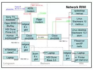
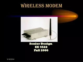
WIRELESS MODEM
WIRELESS MODEM. Senior Design EE 4522 Fall 2000. Team Members. Shane Easterling. Ian Smith. Dr. James Fowler. (Advisor). April Martin. Daniel Ling. Shane Easterling Shane is responsible for creating project web page and packaging. Daniel Ling

WIRELESS MODEM
E N D
Presentation Transcript
WIRELESS MODEM Senior Design EE 4522Fall 2000
Team Members Shane Easterling Ian Smith Dr. James Fowler (Advisor) April Martin Daniel Ling
Shane Easterling Shane is responsible for creating project web page and packaging. Daniel Ling Daniel will be responsible for presenting the preliminary presentation and simulations. April Martin Team Leader April is responsible for presenting the final presentation and building the hardware. Ian Smith Ian is responsible for hardware design and testing. Team Duties
Why Wireless • Today’s businesses are becoming more and more dependent on the internet for means of getting information, buy and selling goods, and conducting business in and around the office. • Wireless offer the following benefits: • Mobility: Access to real-time information anywhere at anytime. The mobility to support productivity and service opportunities not at all possible with wireless networks. • Installation speed and simplicity: Wireless networks are much faster to install and eliminate the need for cable pulling.
Problem Statement • Conventional modem connections requires wiring therefore confining the users to a limited range. • Conventional wireless modems usage does not provide efficient security against unwanted users, and intentional and unintentional interference. • Users obtain slow data rates using the conventional wireless modem.
Objective and Features • Low cost, short range point to point wireless link • Utilize Direct Sequence Spread Spectrum • Meet FCC part 15 operation in the 902-928 MHz band(no end user license required because of using DSSS) • Will be for internal use, providing connection wherever there is a Tx/Rx. Tx will have output power of 1watt (30dBm). • Provide throughput of 2Mb/s
Design Objectives • Cost - Building Modem: Approx. $150 - Market Price: Approx. $400 • Size - 6’’ X 4’’ X 3”, Approx 1.5lbs • Power Consumption - Minimum power consumption
Data Signal is Spread Specified Range Signal Received Signal is Despread Data System Structure Signal is Transmitted
Hardware Design • Power supply: was designed to output 5VDC and –5VDC, as well as, 3-5 VDC. The modem powered by a 5-10VDC wall adapter .
Power Supply Results • We obtained -4.74VDC and 4.73VDC • We also obtained 3.91VDC • Therefore we met the objective of a power supply of -5VDC and 5VDC. We obtained a value near 3VDC.
Hardware Design • Power supply: was designed to output 5VDC and –5VDC, as well as, 3-5 VDC. The modem powered by a wall adapter which converts 120VAC to 5 - 10VDC. • Despreader and LPF:The PLL was design to despread the received signal this is done as soon as possible to determine the RSSI and the PN code.
Calculations • Tcr= 1/Fcr , where Tcr is PN code chip duration and Fcr is chipping rate * let Fcr = 64 Mchips/sec; Avg. Chip rate = 32Mchips/sec *let PN code length , N=63 therefore, Tcr = 1/32Mchips/sec = 31ns • Let R1=R2=R=2.2kohms, C1= AC coupling capacitor C1 = 100/(Pi*R*Fcr) = 100/(Pi*2.2k*32E6) = 452pf • Fc, cutoff frequency, for both filters, F1 and F2, must follow the following relationship with Td (data chip duration): Fc1F1 =Fc2F2 = 2/Td; Td = NTcr Td = 63*31E-9 = 1.959us; Fc1F1=Fc2F2=2/1.959us = 1.024uHz
Calculations (cont’) • Find R3 and R4 RSSI max voltage = 49Vdd/60 = 12.25 LSB R4= 4.45R3 let R3 = 1k therefore, R4 = 4.45*1E3 = 4.45kohms
Hardware Design • Power supply: was designed to output 5VDC and –5VDC, as well as, 3-5 VDC. The modem powered by a 5 - 10VDC wall adapter. • Despreader and LPF:The PLL was design to despread the received signal this is done as soon as possible to determine the RSSI and the PN code. • Cost: The overall cost of the system must not exceed $400. Calculated cost:
Component Cost We are 15% below our objective price of $150
Hardware Design • Power supply: was designed to output 5VDC and –5VDC, as well as, 3-5 VDC. The modem powered by a wall adapter which converts 120VAC to 5 - 10VDC. • Despreader and LPF:The PLL was design to despread the received signal this is done as soon as possible to determine the RSSS and the PN code. • Cost: The overall cost of the system must not exceed $400. Outline of cost: • Power Consumption:
Power Consumption • Calculations: Power consumption of overall system: 12W 12/(60s *60min) = 3E-5kW/hr Utility cost: kw/hr is approx. .08cents Cost/hr= 3E-5*.08 = 2.4E-6cents/hr
Hardware Design • Power supply: was designed to output 5VDC and –5VDC, as well as, 3-5 VDC. The modem powered by a 5 - 10VDC wall adapter. • Despreader and LPF:The PLL was design to despread the received signal this is done as soon as possible to determine the RSSI and the PN code. • Cost: The overall cost of the system must not exceed $400. Outline of cost: • Power Consumption: • Size:6’’ x 4’’x 3’’, Approx 1.5lbs
Size Constraints • Our objective was to have a package size of 6’’x 4’’x 3’’. • Our packaging size is 7’’x 5’’x 3’’, approx. 1.5lb • This was because we were not able to get a printed circuit board, but soldered and wire wrapped the circuit. If we had used a PCB, the circuit would fit into desired package.
Hardware Design • Power supply: was designed to output 5VDC and –5VDC, as well as, 3-5 VDC. The modem powered by a 5 - 10VDC wall adapter. • Despreader and LPF:The PLL was design to despread the received signal this is done as soon as possible to determine the RSSS and the PN code. • Cost: The overall cost of the system must not exceed $400. Outline of cost: • Power Consumption: • Size:6’’ x 4’’x 3’’, Approx 1.5lbs • Throughput:2Mbps
Software Calculations • A throughput of 115kbps can be obtained using RS232. • Calculations: • SX043 was programmed with data rate =100kpbs and bit rate=10us • Let PN code length=31 PNVCO=64MHz,Ref. Osc=5MHz • Chipping Rate =(Data Rate)*(PN code) • =(PN VCO)/(n) , where n is an integer • =(100 E3)*(31) • =3.1 MHz • or =(64 E6)/(20) • therefore: =3.2 MHz • Data Rate =103.2 kbps • .
RF Parameters of Tx/Rx • Transmitter:The transmitter design consisted of: Up/Converter Power Amplifier Tx Switch • Receiver: The receiver design consisted of: RX Switch LNA Down Converter Despreader Demodulator
Simulation for Transmitter Down 6dB 2MHz 902MHz 928MHz
Future Aspects • Improve modem gain so it could be used at further distances from the base antenna • Make the overall product smaller using DSP • Improving the synchronization of both the transmitter and receiver in order to increase the security.
Acknowledgements • We would like to thank Dr. Fowler, our advisor, for all of his valuable input on our project. • We also would like to thank AMIS for providing us with data sheets and parts.