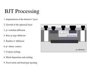
BJT Processing
BJT Processing. 1. Implantation of the buried n + layer. 2. Growth of the epitaxial layer. 3. p + isolation diffusion. n + layer. p + layer. n + layer. 4. Base p-type diffusion. p-base layer. 5. Emitter n + diffusion. n + buried layer. 6. p + ohmic contact. p-substrate.

BJT Processing
E N D
Presentation Transcript
BJT Processing 1. Implantation of the buried n+ layer 2. Growth of the epitaxial layer 3. p+ isolation diffusion n+ layer p+ layer n+ layer 4. Base p-type diffusion p-base layer 5. Emitter n+ diffusion n+ buried layer 6. p+ ohmic contact p-substrate 7. Contact etching 8. Metal deposition and etching 9. Passivation and bond pad opening
BJT Processing 1. Implantation of the buried n+ layer 2. Growth of the epitaxial layer 3. p+ isolation diffusion 4. Base p-type diffusion 5. Emitter n+ diffusion 6. p+ ohmic contact 7. Contact etching 8. Metal deposition and etching p-substrate 9. Passivation and bond pad opening
BJT Processing 1. Implantation of the buried n+ layer 2. Growth of the epitaxial layer 3. p+ isolation diffusion 4. Base p-type diffusion 5. Emitter n+ diffusion 6. p+ ohmic contact n epi layer 7. Contact etching n+ buried layer 8. Metal deposition and etching p-substrate 9. Passivation and bond pad opening
BJT Processing 1. Implantation of the buried n+ layer p+ isolation layer p+ isolation layer 2. Growth of the epitaxial layer 3. p+ isolation diffusion 4. Base p-type diffusion 5. Emitter n+ diffusion 6. p+ ohmic contact 7. Contact etching n+ buried layer 8. Metal deposition and etching p-substrate 9. Passivation and bond pad opening
BJT Processing 1. Implantation of the buried n+ layer p+ isolation layer p+ isolation layer 2. Growth of the epitaxial layer 3. p+ isolation diffusion 4. Base p-type diffusion 5. Emitter n+ diffusion 6. p+ ohmic contact p-base layer 7. Contact etching n+ buried layer 8. Metal deposition and etching p-substrate 9. Passivation and bond pad opening
BJT Processing 1. Implantation of the buried n+ layer p+ isolation layer p+ isolation layer 2. Growth of the epitaxial layer 3. p+ isolation diffusion 4. Base p-type diffusion 5. Emitter n+ diffusion n+ layer n+ layer 6. p+ ohmic contact p-base layer 7. Contact etching n+ buried layer 8. Metal deposition and etching p-substrate 9. Passivation and bond pad opening
BJT Processing 1. Implantation of the buried n+ layer p+ isolation layer p+ isolation layer 2. Growth of the epitaxial layer 3. p+ isolation diffusion 4. Base p-type diffusion 5. Emitter n+ diffusion n+ layer p+ layer n+ layer 6. p+ ohmic contact p-base layer 7. Contact etching n+ buried layer 8. Metal deposition and etching p-substrate 9. Passivation and bond pad opening
BJT Processing 1. Implantation of the buried n+ layer 2. Growth of the epitaxial layer p+ isolation layer 3. p+ isolation diffusion 4. Base p-type diffusion 5. Emitter n+ diffusion n+ layer p+ layer n+ layer 6. p+ ohmic contact p-base layer 7. Contact etching n+ buried layer 8. Metal deposition and etching p-substrate 9. Passivation and bond pad opening
BJT Processing 1. Implantation of the buried n+ layer 2. Growth of the epitaxial layer p+ isolation layer 3. p+ isolation diffusion 4. Base p-type diffusion 5. Emitter n+ diffusion n+ layer p+ layer n+ layer 6. p+ ohmic contact p-base layer 7. Contact etching n+ buried layer 8. Metal deposition and etching p-substrate 9. Passivation and bond pad opening
BJT Processing 1. Implantation of the buried n+ layer 2. Growth of the epitaxial layer p+ isolation layer 3. p+ isolation diffusion 4. Base p-type diffusion 5. Emitter n+ diffusion n+ layer p+ layer n+ layer 6. p+ ohmic contact p-base layer 7. Contact etching n+ buried layer 8. Metal deposition and etching p-substrate 9. Passivation and bond pad opening
Modifications to a BJT Process Dielectric isolation --- substrate isolation Superbeta transistors Double diffusion --- make acceptable JFETs Ion implanted JFETs --- make good JFETs Double diffused pnp BJTs --- make good pnp devices