Download
1 / 26
330 likes | 650 Vues
Outlines. History of Conjugated Polymers Electronic Structures of Conjugated Polymers Polymer Light-emitting Diodes Polymer-based Thin Film Transistors Polymer-based Photovoltaics Polymers for Memory devices. Device Applications of Donor-Acceptor Conjugated Polymers in My Group.

E N D
Outlines • History of Conjugated Polymers • Electronic Structures of Conjugated Polymers • Polymer Light-emitting Diodes • Polymer-based Thin Film Transistors • Polymer-based Photovoltaics • Polymers for Memory devices
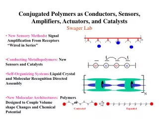
Device Applications of Donor-Acceptor Conjugated Polymers in My Group Al or Au Polymers ITO glass Polymer Solar Cells Polymer Light-emitting Diodes Polymer Thin Film Transistors Polymer Memory Devices
Polymer Based Memory Devices Kang, Polymer 2007; Prog. Polym. Sci.2008 • ON/OFF current ratio (higher value with minimal misreading error; >104) • Switching (write or erase) time (~ms) and read time (~100 ns) • Retention ability (> 1 day) • Programmable (or WRER) cycles (>103 cycles) • Long term stability under voltage stress or read pulse (>107 times) Basic Parameters 3
Polymer Based Memory Devices (Literature) Volatile DRAM DRAM SRAM Non-Volatile WORM Flash Kang, Polymer 2007, 33, 917 Prog. Polym. Sci. 2008, 33, 917 4
Introduction to Computer Memory Computer memory refers to devices that are used to store data or programs (sequences of instructions) on a temporary or permanent basis for use in an electronic digital computer. Computers represent information in binary code, written as sequences of 0s and 1s. Each binary digit (or "bit") may be stored by any physical system that can be in either of two stable states, to represent 0 and 1. Such a system is called bistable. This could be an on-off switch, an electrical capacitor that can store or lose a charge, a magnet with its polarity up or down, or a surface that can have a pit or not. Computer memory is usually referred to the semiconductor technology that is used to store information in electronic devices.There are two main types of memory: Volatile and Non-volatile. An electronic memory is fast in response and compact in size, and can be connected to a central processing unit. Volatile memory: lose the stored data as soon as the system is turned off. It requires a constant power supply to retain the stored information. Non-volatile memory: retain the stored information even when the electrical power has been turned off.
Classification of Electronic Memories ROM (Read-Only Memory) WROM (Write-Once Read-Many Times): CD-R or DVD±R EPROM (Erasable ProgrammableRead-Only Memory) EEPROM (Electrically Erasable ProgrammableRead-Only Memory) FeRAM (Ferroelectric Random Access Memory) Flash: DPA, mobile PC, video player and digital camera DRAM (Dynamic Random Access Memory): As real capacitors have a tendency to leak electrons, the information eventually fades unless the capacitor charge is refreshed periodically. SRAM (Static Random Access Memory): it does not need to be periodically refreshed, as SRAM uses bistable latching circuitry to store each bit.
Fully Printed Passive Array Memories By Thin Film Electronics
Organic Memory Devices Small Molecules Adv Mater 2007, 19, 1452 Polymer Mobile Ion Nanoparticle Blend D-A Complex
Introduction to Memory Devices Capacitor-type Resistor-type Transistor-type The capacitor stores charges, of opposite sign, on two parallel plate electrodes. Each bit of data is stored in a separated capacitor Charge storage and polarization in the dielectric layer or interface of an OTFTs Data storage is based on the high and low conductivity states (electrical bistability) of resistor in response to the applied electric filed Performance factors of RRAM: filamentary conduction, space charges and traps, charge transfer effects, conformation changes, polymer fuse effects, ionic conduction., tunneling.
Basic electric characteristics of Resistor-type Memory Application of a sufficient electric field to an insulator can eventually lead to a deviation from linearity in the resultant current response including (i) threshold switching (ii) memory switching (iii) electrical hysteresis (iv) rectifying (v) negative differential resistance (NDR) (ii) & (iii) have bistability in a voltage or current range Basic Parameters • ON/OFF current ratio • Switching (write or erase) time and read time • Retention ability for non-volatile memory • Programmable (or WRER) cycles • Long term stability under voltage stress or read pulse • Power consumption and cost
Mechanism of Resistor-type Memory Filamentary conduction Metallic filament resulting from local fusing, migrating or sputtering electrode trough the film Trapping & De-trapping Charge Transfer (CT) Effect
Resistor-type Memory: Filamentary Conduction Mechanisms If filaments are formed in a device, (i) the ON state current will exhibit metallic I-V characteristics and will increase as the temperature is decreased and (ii) the injection current will be insensitive to device area or show a random dependence because the dimension is much smaller when compare to the device area. Filament formation and switching effect The filament occurrence depends on three parameters: electrode thickness, film thickness, and the nature of the forming atmosphere.
Resistor-type Memory: Filamentary Conduction Mechanisms Doping-PANI semiconducting polymers Fast switching response ~ 80 ns Reliability test ON/OFF ratio: 103 ITO/P/Al Symmetrical switching ON/OFF ratio: 105 Au/P/Au -3 V bias The localized spots may play as filaments that can be conducted by applied voltage higher than Vt(ON) Adv Funct Mater 2007, 17, 2637
Resistor-type Memory: Filamentary Conduction Mechanisms PS(46900)-b-P4VP (20600) lower erasing voltage ON/OFF ratio: 105 30nm P4VP domain PS display a low current indicating a insulator P4VPcontains pyridiyl groups, interacts strongly with Al. Al atoms migrate into P4VP zones to form metallic filaments. The nanodomain of P4VP in PS-b-P4VPlimit the growth of Al filament whereas the P4VP homopolymer have no limitation to the extent of growth of Al filament. Filament of lager size would be more difficult to break. No significant change after 104 sec Appl Phys Lett 2008, 93, 203303
Resistor-type Memory: SCLC and Filament Formation Previous Works WORM and DRAM memory characteristics as well as polarity-dependent turn on behavior when thickness of the polymer layer in the devices are varied. ON/OFF ratio: 1010 6F-2TPA PI Short circuit current flow too thin stable filament formation ON/OFF ratio: 1011 too thick unstable local filament formation Thinner film shows lower switching threshold voltages (WROM) 15 Nanotechnology 2009, 20, 135204 100 nm thick shows DRAM characteristics
Resistor-type Memory: Space Charges and Traps SCLC operation mechanism Angew Chem Int Ed 2006, 45, 2947 Energy level of LUMO& HOMO and work function of electrode (DRAM) fluorene based D-A conjugated copolymers I-V Characteristics Read cycles on the ON and OFF states
Resistor-type Memory: Space Charges and Traps WORM Polymer 2007, 48, 5182; Adv Mater 2005, 17, 455 Mechanism Flash Polymer 2007, 48, 5182; Solid State Lett 2006, 9, 268
Resistor-type Memory: Charge Transfer Effect A charge transfer effect is defined as an electron donor (D)- electron acceptor complex, characterized by electronic transition to a excited states in which there is a partial transfer of electronic charge from the donor to acceptor moiety. Fomation of ion-radical species and charge transfer complex
Molecular Orbitals of the Basic Units and Transition Induced by Electric Field - + • At threshold voltage, one of the electrons transits from the HOMO to the LUMO+2 within D to form an excited state. • Excitation of D consequently promotes intra- or intermolecular CT at the excited state. • CT can occur indirectly from the LUMO+2 of D to the LUMO+1, then to the LUMO of A, or directly from the HOMO to the LUMO+1 and LUMO at the excited state, to form a conductive complex. • The charges can be further segregated under an electric field and then stabilize the CT state. LUMO+2 LUMO+1 e- LUMO A HOMO D excited state LUMO+2 LUMO+1 LUMO A HOMO D charge transfer state LUMO+1 LUMO+2 LUMO+2 LUMO+1 LUMO A HOMO D LUMO ground state HOMO
Resistor-type Memory: Charge Transfer Effect DRAM 3.2 V -2.1 V At the Vt, on electron transits from HOMO to LUMO3 within D to from excited state. CT can occur indirectly from HOMO to LUMO2, then to LUMO of A or directly from HOMO to LUMO2 and LUMO at the excited state to from a conductive CT complex The lower HOMO explain the higher switch ON voltage while smaller dipole moment (2.06D) leads to a more stable CT structure J Am Chem Soc 2006, 127, 8733
Resistor-type Memory: Charge Transfer Effect Dipole moment: 5.83 Debye (-5.55, -2.04) eV ITO/APTT-6FDA/Al (flash memory) WRER cycles 1.5 V ON/OFF ratio: 104 Form stable CT complex Polarized charge transfer Macromolecules 2009, 42, 4456
Resistor-type Memory: Charge Transfer Effect Dipole moment: 6.00 Debye (-5.71, -2.25) eV ITO/3SDA-6FDA/Al (flash memory) WRER cycles 2.5 V ON/OFF ratio: 104 Large dipole moment Macromolecules 2009, 42, 4456
I-V curves of PI(AAPT-6FDA) (DRAM) W. C. Chen, Macromolecules 2010, 43, 1236 PI(AAPT-6FDA) (D-L-A)n 3&5 : less than 30s after turning off the power A L D I-V curves of PI(APT-6FDA) (SRAM) 2.65 Deybe (-4.92, -2.26) L PI(APT-6FDA) (L-D-L-A)n 3&6 : 4min after turning off the power A L D 2.87 Deybe (-4.87, -2.26) • Weak dipole moment provides an unstable CT complex for the volatile memory device. • The dual-mediated phenoxy linkages of PI(APT-6FDA) produced a potential barrier for delaying the back charge transfer (CT) process by the electric field. ON/OFF ratio > 108 23
Resistor-type Memory: Intramolecular CT Effect AzoONO2(flash) AzoOOCH3 (WORM) When the terminal moieties of azobenzene chromophore are acceptors, trapped charges are stabilized by ICT from a charge separated state. The filled traps may be easily detrapped under reverse bias, resulting in a high conductivity state for a long time in nitro and bormo containing azobenzene. donor acceptor ON/OFF ratio: 104-106 Azobenzene chromophore containing donor are not able to undergo ICT state and the trapped charges can be detrapped by reverse bias AzoNErBr (flash) AzoNEtOCH3 (WORM) ACS Appl Mater & Interface 2009, 1, 60
Resistor-type Memory: Conformational Effects Regiorandom structure Face-to-face regioregular structure