
2 m
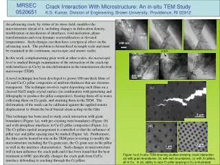
(a). 01-1. 100 nm. 01-1. crack. 2 m. (b). 2 m. 100 nm. (c). 2 m. (d). Figure 1a-d: In-situ TEM straining studies showing crack interaction (a) with grain boundaries, (b) with twin boundaries, (c) with Cr pillars,

2 m
E N D
Presentation Transcript
(a) 01-1 100 nm 01-1 crack 2 m (b) 2 m 100 nm (c) 2 m (d) Figure 1a-d: In-situ TEM straining studies showing crack interaction (a) with grain boundaries, (b) with twin boundaries, (c) with Cr pillars, all in Cu. In (d), ability to vary Cr pillar spacing in Cu is illustrated. MRSEC 0520651 Crack Interaction With Microstructure: An in-situ TEM StudyK.S. Kumar, Division of Engineering, Brown University, Providence, RI 02912 An advancing crack, by virtue of its stress field, modifies the microstructure ahead of it, including changes in dislocation density, modification or decohesion of interfaces, void nucleation, phase transformation and even dynamic recrystallization at elevated temperatures. Such changes can then have a reciprocal effect on the advancing crack. The problem is hierarchical in length scale and must be examined at the continuum, mesoscopic and atomic scales. In this work, complementing prior work at other scales, the mesoscopic level is studied through examination of the interaction of the crack-tip with interfaces in Cu by in-situ deformation in the transmission electron microscope (TEM). A novel technique has been developed to grown 100-nm thick films of Cu and Cu-Cr pillar composites of uniform thickness that are electron-transparent. The technique involves vapor depositing such films on a cleaved NaCl single crystal surface (in combination with patterning and lithography to produce the pillar composites), floating them off in water, collecting them on Cu grids, and straining them in the TEM. The deformation of the mesh can be calibrated against the applied remote displacement to obtain the local biaxial strain acting on the film. This technique has been used to study crack interaction with grain boundaries (Figure 1a), with pre-existing twin boundaries (Figure 1b) and with interphase interfaces in Cu-Cr pillar composites (Figure 1c). The Cr pillars spatial arrangement is controlled so that the influence of pillar size and pillar spacing may be studied (Figure 1d). Furthermore, the film can be heated in-situ in the TEM prior to testing to modify the microstructure including the Cu grain size, the Cr grain size in the pillar as well as the interface characteristics. Such changes in microstructure will in turn influence the crack path and it has been found that the heat treatment at 600C specifically changes the crack path from Cr/Cu interface debonding to cracking through the Cr pillars.