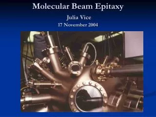
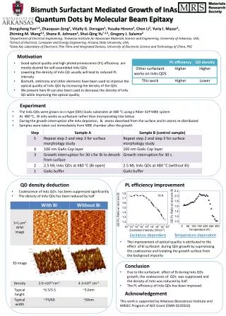
Download
1 / 26
310 likes | 540 Vues
InN Growth by Molecular Beam Epitaxy. Michael Sattler Mentor: Dr. Greg Salamo Post Doc: Dr. Morgan Ware Graduate Student: Eric DeCuir Microelectronic-Photonics REU University of Arkansas July 22, 2008. Presentation Outline. Introduction Experimental Design Results Conclusions

E N D
InN Growth by Molecular Beam Epitaxy Michael Sattler Mentor: Dr. Greg Salamo Post Doc: Dr. Morgan Ware Graduate Student: Eric DeCuir Microelectronic-Photonics REU University of Arkansas July 22, 2008
Presentation Outline • Introduction • Experimental Design • Results • Conclusions • Acknowledgements
Why is InN interesting? • InN has a direct bandgap in the near infrared energy • Can be used with GaN as an alloy to cover the entire visible solar spectrum • Preliminary experiments have demonstrated novel three dimensional growth Perfect matching of band gap of In1-xGaxN to solar spectrum LBNL, 2002 Literature Energy (eV) GaInP GaAs Ge Solar Flux (1021 photons/sec/m2/mm) Ga content in In1-xGaxN alloy
How we grow InN? • Molecular Beam Epitaxy (MBE) • Ultra-high vacuum • Cells containing metals • Radio frequency (Rf) plasma nitrogen source • Sapphire (Al2O3) substrates • RHEED (reflection high energy electron diffraction)
Tools for Analysis RHEED • Reflection High Energy Electron Diffraction • Used to characterize the surface of a sample • Streaky – flat surface • Spotty – three dimensional surface XRD • X-Ray Diffraction • Gives information or crystalline quality • Non-Destructive to material • AFM • Atomic Force Microscope • Very high resolution picture of surface
Project Goals • Learn how to use equipment: • MBE (with RHEED) • XRD • AFM • Gain a better understanding of what growth conditions (substrate temperature and In/N flux) yield 2-D and 3-D growth modes
Growth Procedure • Heat treatment of substrate at ~615°C for 1hr • Helps maintain a constant Tsub during growth • Gallium nitride (GaN) buffer layer: 20 minutes at 760°C • Substrate temperature lowered to desired growth temperature manually (350°C, 400°C, 450°C) • Indium Nitride (InN) growth for 1 hr InN layer (~267 nm) GaN buffer layer (~81 nm) GaN buffer layer (~3 μm) Sapphire substrate (Al2O3) Not to scale
Three-Dimensional Growth Post GaN growth (~81 nm) AFM image ( 1μm) Post InN growth (~267 nm)
Atomically Flat Surface Post GaN growth (~81 nm) AFM image ( 1μm) Post InN growth (~267 nm)
Surfaces of Samples by AFM (1 μm) 10.301 nm 20.322 nm 30.369 nm 116.411 nm 113.739 nm 4.591 nm 110.29 nm 67.812 nm 101.958 nm 4.145 nm 444.162 nm 451.014 nm
XRD • GaN oriented • Various Full Width at Half Maximum (FWHM) is assumed to be from varying lattice orientation instead of bad crystal quality
Full-Width at Half Maximum • Lower FWHM means better crystal quality • Higher FWHM means more defects in the crystal • From the data for a given flux ratio, the lower temperatures show better bulk crystal quality
X-ray Intensity • Slight increase with rising substrate temperature for a given In/N flux • Going to use data to plot the strain in the material for the different samples
Conclusions Trained to effectively use experimental equipment Several samples of InN were grown successfully Gained knowledge of how growth parameters effect the growth modes of InN Don’t mix gallium with an aluminum turbo pump!
Future Studies • Finish original plan in finding the growth transition from 3-D to 2-D at 450°C and 500°C • Find In/N flux that results in a flat surface that lacks indium metal droplets • Temperature dependence photoluminescence 692 meV
Acknowledgements Dr. Greg Salamo Dr. Morgan Ware Eric DeCuir Dr. Omar Manasreh Ken Vickers Renee Hearon National Science Foundation University of Arkansas Arkansas State University
XRD Intensity • Higher intensity is better quality material • From the data for a given substrate temperature, as the In/N flux increases the intensity increases
Gapolar N polar Polarity 11 12