Lecture 3
Lecture 3. OUTLINE Semiconductor Basics (cont’d) Carrier drift and diffusion PN Junction Diodes Electrostatics Capacitance Reading: Chapter 2.1-2.2. Recap: Drift Current. Drift current is proportional to the carrier velocity and carrier concentration :. Total current J p,drift = Q/t

Lecture 3
E N D
Presentation Transcript
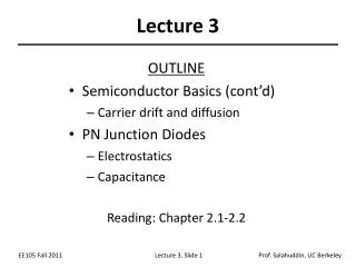
Lecture 3 OUTLINE • Semiconductor Basics (cont’d) • Carrier drift and diffusion • PN Junction Diodes • Electrostatics • Capacitance Reading: Chapter 2.1-2.2
Recap: Drift Current • Drift current is proportional to the carrier velocity and carrier concentration: Total current Jp,drift= Q/t Q= total charge contained in the volume shown to the right t= time taken by Q to cross the volume Q=qp(in cm3)X Volume=qpAL=qpAvht Hole current per unit area (i.e. current density) Jp,drift = qpvh
Recap: Conductivity and Resistivity • In a semiconductor, both electrons and holes conduct current: • The conductivity of a semiconductor is • Unit: mho/cm • The resistivity of a semiconductor is • Unit: ohm-cm
V I _ + W t homogeneously doped sample L Resistance (Unit: ohms) where r is the resistivity Electrical Resistance
Carrier Diffusion • Due to thermally induced random motion, mobile particles tend to move from a region of high concentration to a region of low concentration. • Analogy: ink droplet in water
Carrier Diffusion • Current flow due to mobile charge diffusion is proportional to the carrier concentration gradient. • The proportionality constant is the diffusion constant. Notation: Dp hole diffusion constant (cm2/s) Dn electron diffusion constant (cm2/s)
Diffusion Examples • Non-linear concentration profile varying diffusion current • Linear concentration profile • constant diffusion current
Diffusion Current • Diffusion current within a semiconductor consists of hole and electron components: • The total current flowing in a semiconductor is the sum of drift current and diffusion current:
The Einstein Relation • The characteristic constants for drift and diffusion are related: • Note that at room temperature (300K) • This is often referred to as the “thermal voltage”.
The PN Junction Diode • When a P-type semiconductor region and an N-type semiconductor region are in contact, a PN junction diode is formed. VD – + ID
Diode Operating Regions • In order to understand the operation of a diode, it is necessary to study its behavior in three operation regions: equilibrium, reverse bias, and forward bias. VD = 0 VD < 0 VD > 0
Carrier Diffusion across the Junction • Because of the differences in hole and electron concentrations on each side of the junction, carriers diffuse across the junction: Notation: nn electron concentration on N-type side (cm-3) pn hole concentration on N-type side (cm-3) pp hole concentration on P-type side (cm-3) np electron concentration on P-type side (cm-3)
Depletion Region • As conduction electrons and holes diffuse across the junction, they leave behind ionized dopants. Thus, a region that is depleted of mobile carriers is formed. • The charge density in the depletion region is not zero. • The carriers which diffuse across the junction recombine with majority carriers, i.e. they are annihilated. quasi-neutral region quasi-neutral region width=Wdep
Some Important Relations Energy=-qV
The Depletion Approximation Because charge density ≠ 0 in the depletion region, a large E-field exists in this region: In the depletion region on the N side: r(x) In the depletion region on the P side: qND a -b x -qNA
PN Junction in Equilibrium • In equilibrium, the drift and diffusion components of current are balanced; therefore the net current flowing across the junction is zero.
Built-in Potential, V0 • Because there is a large electric field in the depletion region, there is a significant potential drop across this region: (Unit: Volts)
Built-In Potential Example • Estimate the built-in potential for PN junction below. • Note that N P NA = 1015 cm-3 ND = 1018 cm-3
PN Junction under Forward Bias • A forward bias decreases the potential drop across the junction. As a result, the magnitude of the electric field decreases and the width of the depletion region narrows. r(x) qND a -b x -qNA ID V(x) V0 -b a x 0

