Chapter06
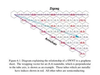
Figure 6.1. Diagram explaining the relationship of a SWNT to a graphene sheet. The wrapping vector for an (8,4) nanotube, which is perpendicular to the tube axis, is shown as an example. Those tubes which are metallic have indices shown in red. All other tubes are semiconducting.

Chapter06
E N D
Presentation Transcript
Figure 6.1. Diagram explaining the relationship of a SWNT to a graphene sheet. The wrapping vector for an (8,4) nanotube, which is perpendicular to the tube axis, is shown as an example. Those tubes which are metallic have indices shown in red. All other tubes are semiconducting.
Figure 6.2. Illustration of the molecular and supramolecular structures associated with nanotubes at three different length scales. (a) shows the wrapping of a graphene sheet into a seamless SWNT cylinder. (b) and (c) show the aggregation of SWNTs into supramolecular bundles. The cross-sectional view in (c) shows that the bundles have triangular symmetry. (d) A MWNT, another nanotube polymorph composed of concentric, nested SWNTs. (e) At the macromolecular scale, bundles of SWNTs are entangled.
Figure 6.3. (a) The unit cell of graphene, and (b) the corresponding reciprocal lattice and Brillouin zone construction by the perpendicular bisector method. Dimensions are not to scale, but orientation between the real and reciprocal lattice is preserved. Important locations within the Brillouin zone are at the zone center, K at the zone corner, and M at the midpoint of the zone edge.
Figure 6.4. The dispersion surface of two-dimensional graphene in proximity to the Fermi level. The valence and conduction bands are tangent at each K point. (From Ref. 48 by permission of the American Physical Society.)
Figure 6.5. (a) Wrapping vectors and allowed k-states for (3,0) (zigzag), (4,2), and (3,3) (armchair) SWNTs. The degeneracy at the K point is allowed only for the (3,0) and (3,3) tubes, which behave like metals. The (4,2) tube does not contain the degeneracy, so it has a band gap. Note that the lines of allowed k-states are perpendicular to the wrapping vector for each tube. (From Ref. 49 by permission of Annual Reviews.) (b) The band structure of a (6,6) SWNT. The presence of many overlapping subbands is typical for SWNTs. (From Ref. 14 by permission of the American Physical Society.)
Figure 6.6. DOS for three metallic and three semiconducting SWNTs. The Fermi level is at 0, and the DOS for the metallic tubes are offset by 0.03 along the vertical axis. Notice that the DOS is zero at EF for the semiconducting tubes but finite for the metallic tubes. For all SWNTs, singularities arise at each band edge due to the low dimensionality of the material. (See Question 1.) (From Ref. 50 by permission of Macmillan MagazinesLtd.)
Figure 6.7. Calculated phonon spectra and PDOS for (5,5), (9,0), and (8,2) SWNTs. The large number of subbands is due to the complexity of the unit cell. The (8,2) tube has the lowest symmetry, corresponding to the largest number of vibrational degrees of freedom and the most complicated phonon spectrum. (From Ref. 15 by permission of Elsevier Science Ltd.)
Figure 6.8. Important vibrational modes in SWNTs, illustrated for a (10,10) SWNT. (a) Longitudinal acoustic mode. (b) Transverse acoustic mode (doubly degenerate). (c) Twisting (acoustic) mode. (d) E2g(2) mode (doubly degenerate). (e) A1g mode (radial breathing mode). Calculated sound velocities are indicated for the acoustic modes, (a-c). (d-e) are Raman active optical modes. (From Ref. 52 with kind permission of Z. Benes.)
Figure 6.9. Mastercurve showing the relationship between RBM frequency and diameter for both calculated (hollow symbols) and empirical (solid symbols) data. (From Ref. 15 by permission of Elsevier Science Ltd.)
Figure 6.10. Time evolution of plasticity in a (10,10) SWNT under 10% uniaxial strain after (a) 1.5 ns, (b) 1.6 ns, and (c) 2.3 ns. The 5-7-7-5 defect is seen to glide apart into separate 5-7 pairs. In (c), it can be seen in the lower 5-7 pair that a second bond rotation has led to the formation of a 5-7-5-8-5 defect. (From Ref. 16 by permission of the American Physical Society.)
Figure 6.11. Illustration of the four primary approaches for synthesizing carbon nanotubes: (a) pulsed laser vaporization, (b) arc discharge, (c) catalytic decomposition, and (d) chemical vapor deposition.
Figure 6.12. Illustration of proposed, atomistic growth mechanisms. (a) Root growth. Growth occurs at the nanotube-catalyst interface, and the tube remains closed at its distal end. (b) Direct addition to strained sites (pentagons) at end caps. (c) Open-ended growth by the ‘scooter’ mechanism. Carbon addition is to dangling bonds, and a migrating, chemisorbed metal catalyst particle (or atom) inhibits spontaneous closure. (d) Illustration of the lip-lip interactions that stabilize MWNT against closure during growth. Carbon addition is to dangling bonds.
Figure 6.13. Transmission electron micrograph (see section 6.4.2.1) of raw nanotube material produced by arc discharge. The multicomponent reaction product includes (1) isolated SWNTs, (2) SWNT ropes, (3) amorphous or uncatalyzed carbons, (4) residual catalyst particles, and (5) polyaromatic graphitic shells. (From Ref. 53.)
Figure 6.14. (a) Simulated electron diffraction pattern of an isolated (10,10) SWNT at normal incidence (e.g. with the electron beam perpendicular to the tube axis). (From Ref. 19 by permission of IOP Publishing Ltd.) (b) Empirical electron diffraction pattern from a SWNT bundle. Reflections from both the rope lattice and the graphene lattice are indicated. The circle delineates a region of the pattern outside of which the contrast has been enhanced for clarity. Therefore, the circle is an analysis artifact and is not intrinsic to the pattern. (From Ref. 53.)
Figure 6.15. Powder neutron diffraction patterns of three different nanotube samples. The inset shows Gaussian fits to the strongest rope lattice peak. The feature at Q ~ 1.8 Å-1 in the PLV pattern is attributed to the presence of graphitic shells that survived purification. (From Ref. 25 by permission of Elsevier Science B.V.)
Figure 6.16. Raman spectrum of acid purified nanotube material. The important spectral features are (a) the E2g(2) modes (G-band), (b) the D-band, and (c) the A1gmodes (RBM band). Inset: detail of the RBM band. (From Ref. 53.)
Figure 6.17. Atomic resolution scanning tunneling microscopy image of an individual (11,7) SWNT. The indices are determined by direct measurement of the chiral angle (7°) and diameter (1.3 nm). (From Ref. 28 by permission of Macmillan MagazinesLtd.)
Figure 6.18. Atomic force microscopy image of an isolated SWNT deposited onto seven Pt electrodes by spin-coating from dichloroethane solution. The substrate is SiO2. An auxiliary electrode is used for electrostatic gating. (Reproduced with kind permission of C. Dekker.)
Figure 6.19. Two common reaction schemes for the covalent derivatization of SWNTs: (I) carboxylic acid derivatization, and (II) fluorination. Many variations on these schemes are possible.
Figure 6.20. Transmission electron micrograph of a MWNT filled with Sm2O3. The interlayer separation in the MWNT is c.a. 0.34 nm. Lattice planes in the oxide are clearly seen. (From Ref. 55 by permission of The Royal Society of Chemistry.)
Figure 6.21. (a) Transmission electron micrograph of C60@SWNT. The nanotube is surrounded by vacuum and does not lie on a substrate. The encapsulated fullerenes form a one-dimensional chain with a lattice periodicity of c.a. 1.0 nm. It is possible to obtain diffraction signatures from these structures. (b) False-color transmission electron micrograph of La2@C80@SWNT. Each C80 cage contains two point scattering centers which are the individual La atoms contained within.
Figure 6.22. Differential conductance spectra of a C60 peapod. (a) Conductance versus position (Å) and sample bias (V) for the peapod. Spatially localized modulations are observed only for positive sample bias, i.e. in the unoccupied density of states. The periodicity of these modulations matches the periodicity of the encapsulated fullerenes. (b) and (c) show conductance at constant position and at constant sample bias. (d) Conductance versus position for the same location on the SWNT after the C60 molecules have been shuttled into an empty part of the tube by manipulation with the STM tip. No periodic modulations are observed. (From Ref. 33 by permission of The American Association for the Advancement of Science.)


