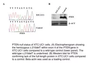
Download
1 / 1
20 likes | 186 Vues
Camera Link (I/O). FPGA. DIO (I/O). AI/AO (I/O). Appropriate I/Os. Development of Flexible and Logic-Reconfigurable VME Boards. T. Hirono, T. Ohata, and T. Kudo JASRI/SPring-8, 1-1-1 Koto, Sayo, Hyogo 678-5198, Japan. Knoxville, Tennessee October 15 – 19, 2007.

E N D
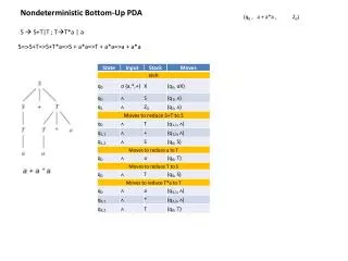
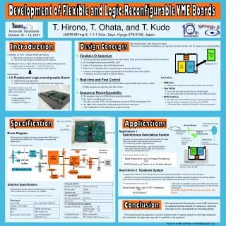
Camera Link(I/O) FPGA DIO (I/O) AI/AO (I/O) Appropriate I/Os Development of Flexible and Logic-Reconfigurable VME Boards T. Hirono, T. Ohata, and T. Kudo JASRI/SPring-8, 1-1-1 Koto, Sayo, Hyogo 678-5198, Japan Knoxville, Tennessee October 15 – 19, 2007 We adopted three main design concepts. These are (1) flexible I/O selection, (2) real-time and fast control, and (3) sequence reconfigurability. Design Concepts Introduction • Flexible I/O Selection • I/O parts physically separated from the base board. They are connected with 64-pin connectors • I/O is simple module such as AI/AO, DIO. • Logic of the sequence are on the base board. • Data from I/O transferred to the base board and processed there. • Software on CPU + Simple AI/AOs and DIOs ○Adjustment of sequences (ex. Adding low-pass filter) ×Fast control that requires microsecond-order response • Hardware in form of hard-wired circuit (ex. ASIC, Analog circuit) ×Adjustments of sequences → A lot of time and cost ○Fast control that requires microsecond-order response → Users of this board can select appropriate I/O boards for their own system or develop only I/O module not whole device. We developed… And also… • I/O Flexible and Logic-reconfigurable Board • Real-time and Fast Control • The base board is mounted with FPGA (field-programmable gate arrays ) chips ○Adjustments of sequences ○Fast control that requires microsecond-order response • VME-bus • VME system, because of the existing system in the SPring-8 • Two FPGA • One for the user logic and the other for the bus control • The user’s logic does not includes logic for the VME-bus control. • DDR memory • User logic can use the DDR memory as temporary data storage • Logic for memory access are in the bus-control FPGA.→User logic dose not affect to the logic for the memory access. → FPGA enables the real-time and fast control The board is suite for a control system with complex sequence that requires fast response. • Sequence Reconfigurability • The sequence are on a FPGA that is reprogrammable. • The logic is modified by the user. The user can edit VHDL source files and recompile FPGA configuration file. • The VME CPU upload the configuration file FPGA to the board For example, • Fast Feedback System • Pattern Driving • Image Processing etc. → The modification of the sequence is quick and easy. Specification Bus-control FPGA Applications User’s ExperimentalSetups Screen Monitor e DIO User FPGA Application 1Synchronous Data-taking System SynchrotronRadiation Camera (Camera Link) Block Diagram Camera Link We developed a flexible and logic-reconfigurable VME board in cooperation with ARKUS Inc*. All the design concepts were implemented. Image Data A system for a new screen monitor that transmits SR beam capture the beam image during user’s experiment. (cf. The existing monitor stops the beam) Analog Data 640 x 480 pixels 12bits/pix 200fps 8 channel Synchronized w/ camera * http://www.arkus.co.jp/index.html →The information about beam , such as beam position and relative intensity, and the data from experiment setups are collected same time. Camera Link(I/O) AI/AO (I/O) Local Bus Configuration Data Outside of the board AI/AO Connector FPGA for I/O control A/D User FPGA The required system is built with Buffer FPGA VME Bus FPGA for VME control Base Board with Logic of Image Processing Isolator VME BusConnector and D/A VME CPU VME system AI/AO Board and Camera Link Grabber Board Connectors The system will be installed with a new screen monitor in March 2008. DDR Interface Application 2 Feedback System I/O Board (AI/AO) Configurator DDR Memory A replacement system for the existing monochromator stabilizer (MOSTAB) of a beamline of the SPring-8 Flash ROM Base Board → Position of the monochromator (an analog input) is feedbacked to stabilize a signal from detector (an analog outputs) that monitors the beam intensity. The sequence is a PID feedback sequence with 10 Hz response. Detailed Specification The required system is built with * We tested the feedback system with PWM outputinstead of analog output. The test was possible because of the flexibility of the board We JUST added PWM-convert logic and a DIO board. Base Board with Logic of PID Feedback and We developed a base board and three types of I/O boards, which are AI/AO,DIO and camera link* grabber. AI/AO Board * * Communication protocol for video products. http://www.machinevisiononline.org/ Conclusion • We designed and developed a new VME board that is characterized by flexible I/O selection, real-time and fast control, and sequence reconfigurability. • The board is/will be applied to control systems with complex sequence and fast response. No hardware change was required to applied to the systems. Author's e-mail address : hirono@spring8.or.jp


![[ t-t-t ]](https://cdn1.slideserve.com/3099327/slide1-dt.jpg)