Download
1 / 67
700 likes | 885 Vues
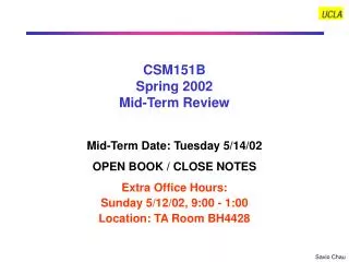
CSM151B Spring 2002 Mid-Term Review. Mid-Term Date: Tuesday 5/14/02 OPEN BOOK / CLOSE NOTES Extra Office Hours: Sunday 5/12/02, 9:00 - 1:00 Location: TA Room BH4428. Areas to Study. What is computer architecture? What is the difference between RISC and CISC? What are their rationales?

E N D
CSM151BSpring 2002Mid-Term Review Mid-Term Date: Tuesday 5/14/02 OPEN BOOK / CLOSE NOTES Extra Office Hours: Sunday 5/12/02, 9:00 - 1:00 Location: TA Room BH4428
Areas to Study • What is computer architecture? • What is the difference between RISC and CISC? • What are their rationales? • How to evaluate computer performance • Execution time calculation • MIPS calculation and pitfalls of MIPS • Concept of Spec Marks • Number Representation • Floating point number representation and IEEE 754 • Floating point operations with IEEE 754 • MIPS instruction set • Able to write simple assembly code with MIPS instruction set • Understanding of procedure calls and stack management • How to implement to single cycle data path and control unit • RTL representation and minimum data path implementation of the instruction • Combining data paths for different instructions • Add control points • Implementing the control unit with logic equation
Areas for Study (continued) • How to add instructions to multi cycle data path • Converting a single cycle data path to multi-cycle data path and what to watch out • Multi-cycle RTL representation of the data path for the instruction • Combining the instruction data path to the main data path • How to design the multi cycle control unit with Explicit Next State Function for an instruction • Finite state diagram for the instruction with control signal values • Combining the instruction finite state diagram to the main finite state diagram • How does the control logic block diagram look like (including inputs & outputs) • Translating finite state diagram into state transition table • Translating state transition table into truth table • Translating the truth table into logic equations • How to design the multi cycle control unit with Micro Sequencer for an instruction • How does the control logic block diagram look like (including inputs & outputs) • How to translate the finite state diagram into the sequence control field • How to generate the dispatch ROMs • Basic idea of micro programming
Control Application ALU Mem I Reg Operating System Software Compiler Firmware Instruction Set Architecture Vdd Instr. Set Proc. I/O system I1 O1 Datapath & Control Vdd I1 O1 Digital Design I2 O2 Hardware I1 O1 Circuit Design Physical Design What is Computer Architecture? • Coordination of many levels of abstraction • Under a rapidly changing set of forces • Design, Measurement, and Evaluation Bottom Up view Courtesy D. Patterson
Seconds Instructions Cycles Seconds CPU time (execution time) = = Instructions Cycles Program Program Performance Analysis Basic Performance Equation: *Note: Different instructions may take different number of clock cycles. Cycle Per Instruction (CPI) is only an average and can be affected by application. Courtesy D. Patterson
Ex Time reference machine Relative MIPS = MIPS reference machine Ex Time target machine Traditional Performance Metrics • Million Instructions Per Second (MIPS) MIPS = Instruction Count / (Time 106) • Relative MIPS • Million Floating Point Operation Per Second (MFLOPS) MFLOPS = Floating Point Operations / (Time 106) • Million Operation Per Second (MOPS) MFLOPS = Operations / (Time 106)
Million Instruction Per Second (MIPS) • Advantage: Intuitively simple (until you look under the cover) • Disadvantages: • Doesn’t account for differences in instruction capabilities • Doesn’t account for differences in instruction mix • Can vary inversely with performance Example: For a 500 MHz machine (5+1+1) 109 (51+12+13) 109 20 sec; = 350 MIPS1 = = CPU Time1 = 20 106 500 106 (10+1+1) 109 (101+12+13) 109 30 sec; = 400 MIPS2 = = CPU Time2 = 30 106 500 106
Exec. Time on Test System Spec Ratio for Each Program = Exec Time on Vax–11/ 780 Specmark = Geometric Mean of all 10 SPEC ratios = n P 10 SPEC Ratio (i) i = 1 1989 SPEC Benchmark • 10 Programs • 4 Logical and Fixed Point Intensive Programs • 6 Floating Point Intensive Programs • Representation of Typical Technical Applications • Evolution since 1989 • 1992: SpecInt92 (6 Integer Programs), SpecFP92 (14 Floating Point Programs) • 1995: New Program Set, “Benchmarks Useful for 3 Years”
Why Geometric Mean? • Reason for SPEC to use geometric mean: • SPEC has to combine the normalized execution time of 10 programs. Geometric means is able to summarize normalized performance of multiple programs more consistently • Disadvantage: Not intuitive, cannot easily relate to actual execution time Example: Compare speedup on Machine A and Machine B B is 10 times faster than A running Program 1, but A is 10 times faster than B running Program 2. Therefore, two computers should have same speedup. This is indicated by the geometric mean but not by the arithmetic mean (in fact, the arithmetic mean will be affected by the choice of reference machine)
IEEE 754 Standard for Floating Point Numbers Two formats: single precision (32-bit) and double precision (64-bit). Single precision format: • Maximize precision of representation with fix number of bits • Gain 1 bit by making leading 1 of mantissa implicit. Therefore, F = 1 + significand, Value = (1)s (1 + significand) 2 E • Easy for comparing numbers • Put sign bit at MSB • Use bias instead of sign bit for exponent field Real exponent value = exponent - bias, bias = 127 for single precision Examples: IEEE 754 value Floating Point Number Value Exponent A = -12600000001 (1)s F 2 (1-127) = (1)s F 2-126 Exponent B = 127 11111110 (1)s F 2 (254-127) = (1)s F 2127 This is much easier to compare than having A = 12610 = 100000102 and B = 12710 = 011111112 • Need to take care special cases (by convention) Value = 0 E = 0 f = 0 i.e., f = significand Value = (1)s E = 255 f = 0 Value = (1)s(0.f)2-126 E = 0 f 0 Value has been denormalized sign Exponent (biased) Significand only (leading 1 is implicit)
IEEE 754 Computation Example A) 40 = (–1)0 1. 25 25 = (–1)0 1.012 2(132 – 127) = [0][10000100][101000000000000000000] B) –80 = (–1)1 1. 25 26 = (–1)1 1. 012 2(133 – 127) = [1][10000101][111101000000000000000] C) By the extended format of the standard, non-normalized significand can be used to align the exponents: 40 = (–1)0 0. 3125 27 = (–1)0 0.01012 2 (134 – 127) = [0][10000110][010100000000000000000] –80 = (–1)1 0. 6250 27 = (–1)1 0.10102 2 (134 – 127) = [1][10000110][101000000000000000000] D) Need to convert the IEEE 754 significand of –80 into 2’s complement before the subtraction: –80 = [1][10000110][101000000000000000000] [1][10000110][011000000000000000000] 40 – 80 = [0][10000110][010100000000000000000] + [1][10000110][011000000000000000000] = [0][10000110][101100000000000000000] E) Convert the result in 2’s complement into IEEE 754 = [1][10000110][010100000000000000000] F) Renormalize: [1][10000110][010100000000000000000] = [1][10000100][010000000000000000000] = (–1)1 1.012 25 Check: 40 – 80 = – 40 = (–1)1 1.25 25 = (–1)1 1.012 25
350 300 RISC 250 200 Performance 150 Intel x86 100 RISC introduction 50 0 1982 1984 1986 1988 1990 1992 1994 Year What is RISC and Why? • RISC is an architecture design concept based on the principle that simpler hardware runs faster (e.g. MIPS). It uses smaller and regular instruction set to achieve performance, while relying on compiler technology to achieve functions used to done by complex instructions. • Opposite to RISC is Complex Instruction Set Computer (CISC) (e.g. Intel x86). CISC believes complex instructions implemented in hardware can reduce the number of memory access and thus achieve higher performance. Language directed architecture such as Burroughs’ B5500 (Algol) or B4500 (Cobol) are extreme cases. Courtesy D. Patterson
The MIPS Instruction Set MIPS is a Reduced Instruction Set Computer (RISC), Characterized By: • It is a Load- Store Machine: Computation Is Done On Data In Registers i. e., Operands of Arithmetic And Logical Operations Do Not ResideIn Memory. Data Is Moved Between Memory And Registers Before Being Used and Back To Memory After Computation Is Finished By Load and Store Instructions • A Relatively Small Number Of Instructions and Data Types • All Instructions Are Of The Same Length • There Are A Very Small Number Of Instruction Formats (3) • There Are A Small Number Of Addressing Modes - Three For Accessing Operands (Register- Direct, Based, Immediate) and One For Computing Jump Addresses (PC- Relative) Courtesy M. Louie
MIPS Instruction Addressing Modes Register (Direct) E.g., add $1, $2, $3 $1$2+$3 OP RS=$2 RT=$3 RD=$1 Register Immediate E.g., addi $1, $2, 100 $1$2 +100 OP RS RT Immediate=100 Base + Index E.g., lw $1, 100($2) $1Mem[$2+100] OP RS=$2 RT Immediate=100 Register Memory PC-Relative E.g., bne $1, $2, 100 Goto Mem[PC+100] if $1=$2 OP RS RT Immediate = 100 PC Memory Psuedo-Direct E.g., J 1000 Goto Mem[PC(31:30):1000] OP Address = 1000 PC Memory
Procedure Calls • Procedure call is used by programmers to structure programs, for easier to understand and reusuability. Example: main() /* This is the calling procedure (caller) */ { funct(100); /* procedure call */ } int funct(arg) /* This is the called procedure (callee) */ { … } • In order to execute procedure call • Step 1:The calling program has to put parameters in a place where procedure can access • Step 2: The calling procedure transfers control to the called procedure while saving the return address at the same time • Step 3: The called procedure executes the desired task • Step 4: The called procedure puts return value in a place where the calling program can access • Step 5: The called procedure returns control to the calling program at the point of origin
MIPS Software Convention for Registers • 0 zeroconstant 0 • 1 atreserved for assembler • 2 v0 expression evaluation & • 3 v1 function results • 4 a0arguments • 5 a1 (calling procedure uses these • 6 a2 registers to pass arguments • 7 a3to the called procedure) • 8 t0 temporary: caller saves • do not need to be preserved across procedure calls • . . . (called procedure can clobber) • 15 t7 • 16 s0 callee saves • need to be preserved across procedure calls • . . . (calling procedure can clobber) • 23 s7 • 24 t8 temporary (cont’d) • 25 t9 • 26 k0reserved for OS kernel • 27 k1 • 28 gp Pointer to global area • holding a program’s static data • 29 sp Stack pointer • 30 fp frame pointer • 31 raReturn Address (HW) • Stack frame -- A block of memory allocated on the stack for the subroutine call environment. • Purpose: • hold values passed as subroutine arguments • save register values that the calling subroutine needs to use after the callee returns • provide space for local variables since there are only a limited number of registers
An Overly Simplified Example Addr main() /* Caller */ { x = y + z; funct(arg); /* procedure call */ … } $v0 w ($2) 1 arg $a0 ($4) 2 funct addr 1 2 main addr main addr 3 1 2 3 PC 3 x w $t0 ($8) 3 y v $t1 ($9) main addr3 $ra ($31) z $t2 ($10) Addr int funct( arg ) /* Callee */ { w = arg – v; return (w); } arg 1 2 3 • But! • What if there are more than 4 arguments? • What if there are some register values need to be preserved across procedure call (e.g., if you want to preserve the value x)? • What if another procedure call happens before the current procedure is completed?
Call-Return Linkage: Stack Frames • Solution: • Save the needed information (e.g., arguments, return address) onto a stack in memory • Information needed by the called procedure are grouped into a stack frame • Many variations on stacks possible (up/down, last pushed / next ) High Mem Reference Arguments and Local Variables at Fixed (negative) Offset From FP FP ARGS (frame pointer points to 1st word of frame) Callee Save Registers (old $fp, $ra, $s0,etc) Stack Frame or Activation Record Local Variables SP (stack pointer points to last word of frame) Grows and shrinks during expression evaluation Low Mem
MIPS Instructions for Procedure Call • MIPS uses a jump and link instruction for procedure calls • Jumps to the address specified in the lower bits of the instruction • Simultaneously save the address of next instruction (i.e. PC+ 4) in the Return Address (RA) register (R31) • Use jump register (jr RA) for return
Five Classic Components of a Computer Processor (CPU) Input Control Memory Datapath Output
Steps to Design a Processor • 5 steps to design a processor • 1. Analyze instruction set => datapath requirements • 2. Select set of datapath components & establish clock methodology • 3. Assemble datapath meeting the requirements • 4. Analyze implementation of each instruction to determine setting of control points that effects the register transfer. • 5. Assemble the control logic • MIPS makes it easier • Instructions same size • Source registers always in same place • Immediates same size, location • Operations always on registers/immediates Datapath Design Cpntrol Logic Design
Step 1: Analyze the Instruction Set Specify Requirements for the Data Path • Where and how to fetch the instruction? • Where are the instructions stored? • Instruction format or encoding • how is it decoded? • Location of operands • where to find the operations? • how many explicit operands? • Data type and Size • Type of Operations • Location of results • where to store the results? • Successor instruction • How to determine the next instruction? • (next address logic for jumps, conditions branches) fetch-decode-execute next address is implicit!
Specifying Datapath Implementation with Register Transfer Languages (RTL) • Specify what state elements (registers, memories, flip-flops) are needed to implement the instructions • Describe how signals are transferred among state elements • There are many types of RTLs. Examples: VDHL and Verilog • An informal RTL is used in this class: Syntax:variable expression Where variable is either a register or a signal or signal group (Note: Use the following convention in this class. Variable is a register if it is all caps or in form of array[address]. Otherwise it is a signal or signal group) Expression is a function of input signals and the output of other state elements • Example: RTL for R-Type Instruction instr mem[PC] Instruction Fetch rs instr<25:21> Define Signals (Fields) of Instr rt instr<20:16> rd instr<15:11> R[rd] R[rs] + R[rt] Add Register Contents PC PC + 4 Update Program Counter
R1 R2 . . . . . . . . . . . . Clk Setup Hold Setup Hold Don’t Care Setup (Hold) - Short time before (after) clocking that inputs can’t change or they might mess up the output Register Transfer Language and Clocking Register transfer in RTL: R2 f(R1) What Really Happens Physically 0 1 1 1 1 0 0 1 1 1 Two possible clocking methodologies: positively triggered or negatively triggered. This class uses the negatively-triggered.
ALU Data Memory addr data in data out Step 3: Assemble the Datapath for Load Operations • lw rt, immed16(rs) Instr <- mem[PC] Instruction Fetch rs <- Instr<25:21> Define Signals (Fields) of Instr rt <- Instr<20:16> imm16 <- Instr<15:0> Addr <- R[rs] + SignExtend(imm16) Calculate Memory Address R[rt] <- Mem[Addr] Load Data into Register PC <- PC + 4 Update Program Counter PC+4 Next Address Logic PC Register File Instruction Memory Rd addr1 Wr addr Wr data mux ext
Inst Memory Instruction<31:0> Adr <21:25> <16:20> <11:15> <0:15> • We Have Everything Except Control Signals (underline) MUX 1 0 Rs Rt Rd Imm16 RegDst nPC_sel ALUctr MemWr MemtoReg Equal Rd Rt Rs Rt 4 RegWr 5 5 5 busA Adder 0 Rw Ra Rb = busW 00 32 32 32-bit Registers rt 0 32 Adder MUX busB 32 PC PC+4 0 32 MUX MUX Clk 32 1 WrEn Adr Adder Data In 1 Clk Data Memory PC Ext Extender imm16 32 1 16 imm16 Clk ExtOp ALUSrc A Complete Single Cycle Data Path and Load Instruction Operations rs PC+4 data for rt
Required Control Signals for the Given Data Path Instruction<31:0> Instruction Memory <0:15> <21:25> <21:25> <16:20> <11:15> Adr Op Fun Rt Rs Rd Imm16 Control Branch Jump RegWr RegDst ExtOp ALUSrc ALUctr MemWr MemtoReg Zero DATA PATH
Step 4: Determine Control Points for the Single Cycle Data Path — Control Signals for Load • R[ rt] Data Memory [R[ rs] + SignExt( imm16)] Branch = 0 Jump = 0 RegDst = 0 ALUctr = ALUctr add RegWr = 1 1 MemtoReg = MemWr = MemWr = 0 0 Mem Data ALUSrc = ExtOP = 1 1
Single Cycle Data Path Control Signals for Branch • If (R[rs] - R[rt] == 0 ) Then Zero 1 ; else Zero 0 Branch = 0 Jump = 0 RegDst = x ALUctr ALUctr = sub Zero RegWr = 0 MemtoReg = x MemWr = 0 ExtOP = x ALUSrc = 0
Instruction Fetch Unit at the End of Branch • If ( Zero == 1 ) Then PC = PC + 4 + SignExt( imm16) * 4 ; Else PC = PC + 4 Jump = 0 Branch = Zero = ExtOP = 1 1 1
Instruction Fetch Unit at the End of Jump • PC PC_incr< 31: 28> concat target< 25: 0> concat “00” Jump = 1 Branch = 0 Zero = x ExtOP = X The data path has nothing to do! Make sure all Write Enable signals are disabled!
Step 5: Assemble the Control Logic A Summary of the Control Signals These signals can easily be expressed as functions of the opcodes See following discussions
Truth Table for ALUctr 26 = 64 words 29 = 512 words op I-type uses the opcodes but not the func field R-type has only 1 opcode but uses the func field for encoding • ALUop = f (opcode) ; as shown in the previous slide • ALUctr = f (ALUop, func)
op[1:0] Binvert Binvert op[1:0] cin a0 a 0 result0 b0 0 0 1 1 1 sum + result b 2 a1 result1 b1 Less sum 3 cin 0 cout a b op[1:0] Binvert cout Cin Cin ALU1 ALU0 cin zero a 0 Less Less Cout Cout Cin 1 ALU31 a31 result31 b31 overflow sum + Less result b 0 2 set Less 3 set overflow Overflow detection Data Path Element: ALU
Logic Equations for the ALUctr Signals This makes func< 3> a don’t care ALUctr<2>: ALUctr<2> = !ALUop<2> & !ALUop<1> & ALUop<0> + ALUop<2> & !ALUop<1> & !ALUop<0> & !func<2> & func<1> & ! func<0> ALUctr<1>: ALUctr<1> = !ALUop<2> & !ALUop<1> + ALUop<2> & !ALUop<1> & !ALUop<0> & !func< 2> ALUctr<0>: ALUctr<0> = !ALUop<2> & ALUop<1> & !ALUop< 0>+ ALUop<2> & !ALUop<1> & !ALUop<0> & !func<3> & func<2> & !func<1> & func<0>+ ALUop<2> & !ALUop<1> & !ALUop<0> & func<3> & !func< 2> & func< 1> & ! func< 0>
Jump R-Type Load Instr decode R read Instr decode R read ALU delay Reg write ALU delay Mem read Reg write PC write Instr Fetch Instr Fetch Instr Fetch Instr Fetch Instr Fetch Instr Fetch Instr decode Time wasted Time wasted Time wasted Clock Clock Clock Clock Jump R-Type Load Instr decode R read Instr decode R read ALU delay Reg write ALU delay Mem read Reg write PC write Instr decode Clocks Problem with Single Cycle Processor Design • The Root of the Single Cycle Processor’s Problem: • The Cycle Time has to be Long Enough for the Slowest Instruction. Time is wasted in short instructions. • This is a serious problem because short instructions occur much more often. • Solution: • Break the Instruction into Smaller Steps • Execute Each Step (Instead of the Entire Instruction) in One Cycle • Cycle Time: Time it Takes to Execute the Longest Step • Keep All the Steps to a Similar Length
Control PC Basic Idea of Multi Cycle Data Path R-type 4 cycles Load 5 cycles Jump 3 cycles MemtoReg nPC_sel PC_Wr ALUctr MemWr ALUSrc IR_Wr MemWr RegDst RegWr ExtOp Reg File mux R A Exec Operand Fetch Instruction Fetch Result Store Next PC IR B M Mem Access Data Mem
Data address Reuse of Function Units in Multi Cycle Data Path • Since intermediate results are stored in intermediate registers, function units can be doing different things at different time Examples: • Memory can be used to store both instructions and data • ALU can be used to do arithmetic and calculate branch address • Price to pay: extra registers (IR, ALUout) and multiplexors IR Load Instruction: PC Mem Data Reg Mem mux Instruction Fetch ALUout Calculate Address mux Read Memory Data PC Reg A PC PC mux 4 4 Reg A Reg file or mem Shift 2 ALUout Reg File Reg B Shift 2 bits for branch mux Reg B Instr IR Need to hold the output so ALU can be reused (15:0) Instruction (15:0) Single Cycle Data Path Multi Cycle Data Path
General Steps to Design Multi Cycle Datapath Step 1: Start with a single cycle data path that is capable to perform all execution steps Step 2: Insert registers after each step in the instruction execution sequence Step 3: Combine components if possible and add multiplexors Step 4: Work out clock by clock control signal sequence Note: Make sure IR is not changed before end of instruction
Step-by-Step Analysis of Multi Cycle Data Path Instruction Execution Sequence • Step 1: Instruction Fetch • Step 2: Instruction Decode and Register Fetch • Step 3: Execution, Memory Address Computation, or Branch Completion • Step 4: R-Type Completion or Memory Access for Load/Store Instructions • Step 5: Memory Read and Load Completion
Cycle Ends AT the Next Clock Tick • IRmem[PC]; PC<31: 0> PC<31: 0> + 4 • Cycle Begins Right AFTER the Clock Tick • Instr Reg mem[PC]; PC<31: 0> + 4 PC+12 PC+8 PC+8 PC+4 Instruction Fetch Step One Clock Cycle ALUOp= Add, ALUSrcB= 01 x: PCWrCond, RegDst, MemtoReg, ExtOp 1: PCWr, IRWr; Others: 0 PC+4
Load Instruction Decode Step OpFetch/Decode ALUOp= Add, ALUSrcB= 11 x: RegDst, PCSrc, IorD, MemtoReg 1: ExtOp Others: 0
Load Instruction Execution Step (Memory Address Calculation)
Load Instruction Completion Steps Skip Forward
Jump Instruction Decode and Complete Steps • • PC_ incr PC + 4 • PC<31: 2> PC_ incr<31: 28> concat target<25: 0> JComplete 1: PCWrite PCsrc = 10 x: others PCWr=1 PCsrc=2 2 1 0 J Instr<25:0> PC<31:28> 4 26
Overview of Control Hardware Development • Control may be designed using one of several initial representations. The choice of sequence control, and how logic is represented, can then be determined independently; the control can then be implemented with one of several methods using a structured logic technique.