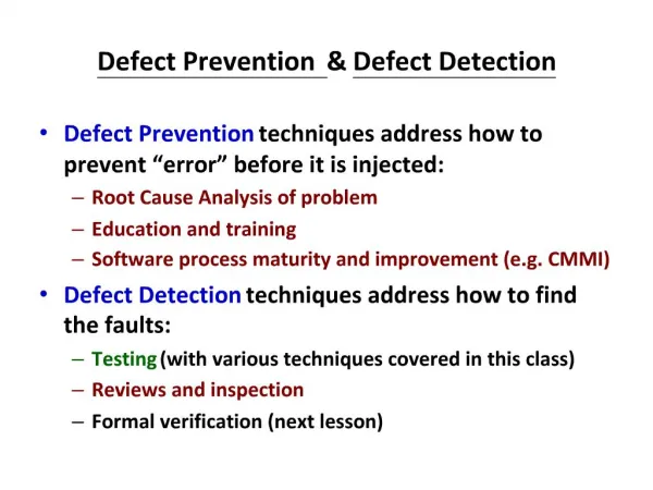
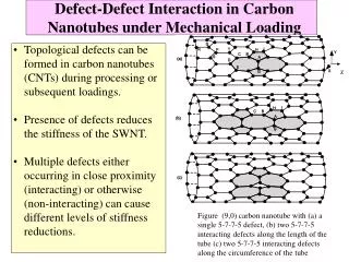
Download
1 / 1
10 likes | 172 Vues
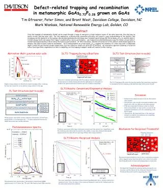
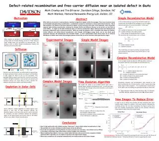
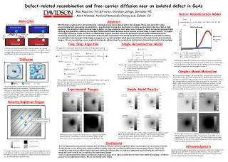
Defect-related recombination and free-carrier diffusion near an isolated defect in GaAs Mac Read and Tim Gfroerer, Davidson College, Davidson, NC Mark Wanlass, National Renewable Energy Lab, Golden, CO. Better Recombination Model. Motivation. Abstract. Defect-related Recombination.

E N D
Defect-related recombination and free-carrier diffusion near an isolated defect in GaAs Mac Read and Tim Gfroerer, Davidson College, Davidson, NC Mark Wanlass, National Renewable Energy Lab, Golden, CO Better Recombination Model Motivation Abstract Defect-related Recombination Radiative Recombination When defects are present in semiconductors, localized energy levels appear within the bandgap. These new electronic states accommodate heat-generating recombination – a problematic energy loss mechanism in many semiconductor devices. But at high excitation, the density of electrons and holes is higher, so they encounter each other more frequently. Early encounters augment light-emitting recombination, reducing the average lifetime and diffusion distance so the carriers are less likely to reach defects. In images of the light emitted by GaAs, we observe isolated dark regions (defects) where the darkened area decreases substantially with increasing excitation. When we modeled the behavior with a simulation that allows for lifetime-limited diffusion and defect-related recombination only through mid-bandgap energy levels, we did not obtain good agreement between the experimental and simulated images. We are now testing a more sophisticated model which allows for an arbitrary distribution of defect levels within the bandgap. Conduction Band Conduction Band - - Defect Level ENERGY HEAT HEAT LIGHT + + Time Step Algorithm Simple Recombination Model Valence Band Valence Band The algorithm to find steady state carrier densities (n) in each pixel follows a simple rate equation including generation, recombination, and Laplacian diffusion: Electrons can recombine with holes in semiconductors by hopping through localized defect states and releasing heat. This defect-related trapping and recombination process is a loss mechanism that reduces the efficiency of many semiconductor devices. Assumptions: * All defect states are located near the middle of the bandgap so we neglect thermal excitation of carriers into bands. Method: We determine the 2 A coefficients (one for the defect pixel and one for the non-defective pixels) that minimizes the error between the measured and simulated efficiencies. Where: Aτ = 1 / defect capture time (1/τ ) dDp = number of trapped electrons dDn = number of trapped holes The density of states (DOS) function now allows for thermal excitation and asymmetric band filling, affecting dP, dN, dDp, and dDn. In our computation, we also adjust the amplitude of the DOS functions to correct for changes with laser focusing (see Caroline Vaughan’s poster!). Diffusion Where: Where: dP = number of electrons in the conduction band dN = number of holes in the valence band n = total number of excited carriers A = defect constant B = radiative constant Low-excitation High-excitation + - + d - Complex Model Motivation - y D y D + + + (Depend on the model) In our experimental images, radiative efficiency increases more rapidly with carrier density than the simple model predicts. By allowing the defect and nondefect A values to change with laser intensity in the simple model, we find that a larger defect A is needed for lower carrier densities (see below). The defect-related recombination model described above can produce a similar effect. At low carrier density, electrons are trapped and defect-related recombination dominates, but when the traps are filled, the radiative efficiency increases rapidly as all new electrons enter the conduction band. - d - • We use Laplacian diffusion to determine the flux between adjacent pixels during each time step and then calculate new carrier densities. • We allow the diffusion process to continue until the average lifetime of the generated carriers is reached. x x D Defect - Electron + Hole The carrier lifetime is determined by how long it takes an electron to find a suitable hole for recombination. At low excitation density, electrons are more likely to encounter a defect before a hole, allowing for defect-related trapping and recombination. At high excitation, the electrons and holes don’t live as long, reducing the diffusion length d and the probability of reaching a defect before radiative recombination occurs. Experimental Images Simple Model Results Density Depletion Region - BigA = 4.2*107 SmA = 8.1*104 - - Using the time step algorithm and the simple recombination model described above , we obtain these theoretical images. The simulated images, with A=4.2*107 cm3/s (defect pixel) and A=8.2*104 cm3/s (non-defect pixels), produced the lowest error in the context of this model. By allowing the A values to change for each laser power, we are able to reproduce the experimental results. These images, using defect A values ranging from 4.2*107 cm3/s to 2*108 cm3/s and non-defect A values from 8.2*104 cm3/s to 1.6*105 cm3/s, show that we need a more sophisticated model for defect-related recombination. Photoluminescence images are obtained from an undoped GaAs/GaInP heterostructure. The excitation intensity-dependent images shown above center on an isolated defect in the thin, passivated GaAs layer. Low density High density A=4.2*107 cm3/s A=8.2*104 cm3/s Conclusions Acknowledgments • Even for high-quality semiconductor materials with few defects, diffusion can lead to significant defect recombination at low excitation intensity. • At low density, carriers diffuse more readily to defective regions rather than recombining radiatively, producing larger effective “dead” areas. • Assigning a single defect coefficient to each pixel and allowing for diffusion does not yield good agreement, but by allowing the coefficient to change with laser intensity, we can reproduce the experimental images. • A more sophisticated defect-related recombination model that allows for an arbitrary distribution of defect levels within the bandgap is needed to account for our experimental results. We are now testing such a model. We thank Jeff Carapella for growing the test structures, and Caroline Vaughan and Adam Topaz for their work on finding the DOS functions. We also thank the Davidson Research Initiative and the Donors of the American Chemical Society – Petroleum Research Fund for supporting this work. We model the defect as an isolated pixel with augmented defect-related recombination. Diffusion to this pixel reduces the carrier density n near the defect, and since the brightness is proportional to the radiative rate Bn2, the adjacent region appears darker. Carrier density is reduced by diffusion to the defect