
Understanding the Datapath and Control Signals in Memory Addressing and Operations
This document provides an in-depth exploration of the datapath and control signals involved in memory addressing and operations within a computational architecture. It details the functionality of various registers, memory blocks, and the Arithmetic Logic Unit (ALU). Instructions like MOV and ADD regarding registers and memory are examined, along with the control outputs needed for each operation. Key considerations include enhancing interrupt handling speed and analyzing propagation delays in the context of pipeline efficiency. Additional queries prompt architectural modifications for optimal performance.

Understanding the Datapath and Control Signals in Memory Addressing and Operations
E N D
Presentation Transcript
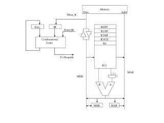
Memory Data Addr R0/PC R1/SP R2/SR R3/CG R4 MDR State Combinational Logic IR R15 MAR B A Mem_B From SR To Datapath MAB MDB
Datapath control signals • Registers file • LD_Rx, x={0..15} – load register x from MDB • OEA_Rx – output register x to ALU A input mux • OEB_Rx – output register x to ALU B input • OE_MAB_Rx – output register x to MAB • Other registers • LD_IR • LD_MDR • LD_MAR • ALU • ALU_op, op= {ADD, SUB, A+1, A^B, …} • LD_SR • ALUOE_x, x={MAB, MDB} • ALU_A_x, x={reg, IR, MDR, …} • Memory • Read – MEMD <- M(MAB) • Write – M(MAB) <- MEMD • OE_MEMD_to_MDB • OE_MDB_to_MEMD
MAB MDB MEMD ALU_A ALU_B LD_IR LD_Rx OEA_Rx OEB_Rx OE_MAB_Rx LD_IR LD_MDR LD_MAR ALU_op LD_SR ALUOE_x ALU_A_x Read Write OE_MEMD_to_MDB OE_MDB_to_MEMD
MOV R5,R6 MOV R5,R0 Next Inst. Cycle 1 Cycle 1 Cycle 1 Cycle2 MAB MDB MEMD ALU_A ALU_B PC0 PC0+2 PC0+4 R5 R5+2 R5 R5 MOV R5,R0 Next inst. R5 R5 LD_Rx INC_PC OEA_Rx OEB_Rx OE_MAB_Rx LD_IR LD_MDR LD_MAR ALU_op LD_SR ALUOE_x ALU_A_x Read Write OE_MEMD_to_MDB OE_MDB_to_MEMD LD_R6 LD_R0 5 5 0 0 A A MDB MDB regfile regfile
Questions • Draw the control outputs and datapath contents for the following instructions • MOV R5, R6 • MOV R5, PC • ADD R5, R6 • ADD R5, PC • ADD @R5, R6 • ADD @R10+, R12 • AND #FF80, R15 • XOR EDE, R9 • JZ R4 (first assume Z=0, then Z=1) • CALL #1234 • Can you execute SUB EDE, TONI with this datapath? If not, how would you modify the datapath to allow it? Either way, draw the control/datapath signals. • Fast interrupt service is very important in some real-time applications. The MSP430 requires 6 cycles between the interrupt and execution of the first instruction of the interrupt handler. RETI (return from interrupt) requires 5 cycles. What architectural changes could you make to speed up interrupt handling? With these changes, what is the fewest number of cycles needed from interrupt to execution of the first interrupt instruction? Fewest number of cycles for RETI? • Assume that the ALU propagation delay is 50ns, memory reads/writes are 50ns, combination logic delay is 10ns, register setup times are 5ns, and register propagation delays are 5ns. What is the minimum clock period for the processor? (I’d be more specific on the test: what’s the minimum clock period to execute 1A above, or 1C, or 1I; which of those instructions contains the cycle with the longest delay, and what is the delay on that critical path?) • Is the datapath controller a Mealy machine or a Moore machine? Why?