Download
1 / 22
220 likes | 340 Vues
Exploring lens-coupled LEKIDs concept, micromachined silicon lenses, titanium nitride growth, and conclusions for future work in submm applications. Electromagnetic simulations, lens fabrication details, and material characterization are highlighted.

E N D
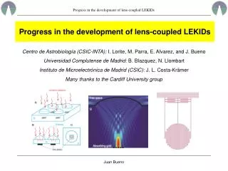
Progress in the development of lens-coupled LEKIDs Centro de Astrobiología (CSIC-INTA): I. Lorite, M. Parra, E. Alvarez, and J. Bueno Universidad Complutense de Madrid: B. Blazquez, N. Llombart Instituto de Microelectrónica de Madrid (CSIC): J. L. Costa-Krämer Many thanks to the Cardiff University group
Outline 1.- Lens-coupledLEKIDs • 2.- Electromagneticsimulations • - Absortionefficiency • - Resonatordesign • 3.- Microfabricatedsiliconlenses • - A simple idea • - Fabrication • Surfacecharacterization • - Beampatternmeasurements • 4.- TitaniumNitride • - Sputteringchamber • - Growth • X-raydiffraction • Ramanspectroscopy • - Hall effect 5.- Conclusions & futurework
Lens coupledLEKIDs: concept • Siliconlensfocusestheradiationontotheinductivepart of the detector • Reduces crosscouplingsincethespacingbetweenthepixelsislarger • Increasesthesamplingefficiencybecausetheradiationisfocusedintotheinductivepart • Disadvantage: • more complicated 3D structure
Electromagneticsimulations:absorptionefficiency (I) • Analyticalmodel • Full-wave simulations (CST) • Efficienciesover 90% in a broad band (from 0.5 to 2.2THz) assumingthatthegrid has aninfinitearea
Electromagneticsimulations:absorptionefficiency (II) • ThelensfocuseswithanAirypattern • Thespilloverdependsonhowmanyfringes of theAirypattern are onthe LEKID • The total efficiencyisover 80% for a broad band from 0.5 to 2.2THz
Electromagneticsimulations:the detector • LEKID isdesignedwith a circular shapeformsamplingthefirsttwofringes of theAirypattern • A 5x5 pixel arrayfor 1.4THz has beendesigned
Micromachined Si lenses: ‘simple’ idea • Deposit a photoresistdroponto a siliconwafer • Transfer theshape of a resistdropintothesiliconwaferby Reactive Ion Etching • Thesiliconlensismade
Micromachined Si lenses:fabrication • Transfer a drop of photoresistintothesiliconbymeans of RIE • Theheigth and width of thedrop can becontrolledwiththedensity of thephotoresist • Currentlydeveloping a methodusinglithographictechniqueswithgoodpreliminaryresults
Micromachined Si lenses:surfacecharacterization (I) • SEM imagestaken • Pittingobservedduetosolventmicrobubbles in thephotoresist • Surfaceroughness of 3mm
Micromachined Si lenses:surfacecharacterization (II) • AFM imagestaken • Porous are 500nm deep • Theareawith no porous has a surfaceroughness of about 100nm
Micromachined Si lenses:surfacecharacterization (II) • Picture of a lenscompletelyetched • Lenseswith a diameterbetween 1.5 – 4.5 mm havebeenfabricated • Theheigth of thelensesvariesfrom 50 to 350 mm
Micromachined Si lenses:beampatternmeasurements (I) • Beam spot at the focus plane of the lens measured using a multiangle knife-edge method • A CO2 laser at 10.6mm wavelegth has been used • 1D are traced to get a 2D image of the beam pattern of the lens at the focal plane
Micromachined Si lenses: beampatternmeasurements (II) • Beampatternmeasured at differentdistancestofind focal plane • Thebeam spot at the focal plane has a diameter of 200mm
TitaniumNitride:sputteringchamber • Home-madesystem, dedicatedchamberfor • TiNgrowth • Load-locksystemforsubstrate transfer • Base pressurebelow 5x10⁻⁹ mbar • 2” Ti target
TitaniumNitride: growth Power: 200W Thickness: 40-125nm Power: 200W Thickness: 40-80nm Power: 200W Thickness: 225nm Power: 200-300W Thickness: 25-125nm New target • Resistivity of 30mW cm for N2concentrationsbetween 5 and 25% • ResistivityevenlowerthantheAluminiumonefor N2concentrationsabove 75%
TitaniumNitride:x-raydifractionmeasurements • Differentlatticestructuredependingonthethickness • Transitionoccursbetween 125 and 225nm • Top graphisconsistentwithVisserset al.paper Tc=1K Tc=3.3K
TitaniumNitride:Ramanspectroscopymeasurements • Superconductingsamples • Non-superconductingsamples • Disorderseemstohelpthesuperconductivity
TitaniumNitride: Hall effectmeasurements • Two films at 15% N2concentration • Resistivity comparable withtheonemeasuredpreviously • Leftplotissuperconducting and rightplotdoesnotsuperconduct • Leftplot: ‘p’ carriers; rightplot: ‘n’ carriers • Number of carriers in theorder of 1023
Conclusions • 1.- Electromagneticsimulations • Absortionefficienciesover 80% over a broad band • A 5x5 pixel arrayreadytobefabricated • 2.- Microfabricated Si lenses • A fairlyinexpensivemethodforlensfabricationwithstandardcleanroomtechniques has beendeveloped • Thelenssurface has a roughness of 3mm, goodenoughforanysubmmapplication • - Thebeampattern has beenmeasuredshowingthatfocuses light • 3.- Titaniumnitride • We are abletogrowsuperconductingTiNwithtunable Tc (0.5 - 4K) and r = 30mW cm • Thelatticechangesdependingonthethickness of thedepositedTiN (somewherebetween 125 and 225nm) • The more disorderedthe film is, thebetter superconductor itbecomes (?) • Differentcarriertypescouldbe a superconductivity trace (?)
Workto do beforethenext KISS workshop 1.- Fabricatethe 5x5 pixel array (nextweek) and measureitwith and withoutlenses 2.- Continuetodevelop a methodforfabrication of biglensarrays 3.- ContinuetheTiNcharacterizationtoobtain a roomtemperaturediagnostictoolthatallowstoknowwhetherthe film issuperconductingbeforecoolingitdown
Anyquestions? Ask my daddy a difficultquestion… . ifyoudare!!!