Abstract
GIEE SPEECH Title: Accurate and efficient modeling of on-chip inductor and on-chip parasitic inductance for SoC designs Speaker: Keh-Jeng Chang, Ph.D. ( 張克正博士 ) Time:3:00-4:00pm, June 2, 2003 (Monday) Place: Room 229, EE#2 Building, National Taiwan University. Abstract

Abstract
E N D
Presentation Transcript
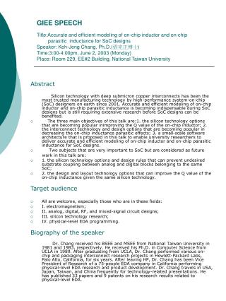
GIEE SPEECHTitle:Accurate and efficient modeling of on-chip inductor and on-chipparasitic inductance for SoC designsSpeaker: Keh-Jeng Chang, Ph.D.(張克正博士) Time:3:00-4:00pm, June2, 2003 (Monday)Place: Room 229, EE#2 Building, National Taiwan University Abstract Silicon technology with deep submicron copper interconnects has been the most trusted manufacturing technology by high-performance system-on-chip (SoC) designers on earth since 2001. Accurate and efficient modeling of on-chip inductor and on-chip parasitic inductance is becoming indispensable during SoC designs but is still requiring extensive research before SoC designs can be benefited. • The three main objectives of this talk are:1. the silicon technology options that are becoming popular inimproving the Q value of the on-chip inductor; 2. the interconnect technology and design options that are becoming popular in decreasing the on-chip inductance parasitic effects; 3. a small-scale software architecture that is proposed in this talk to enable university researchers to deliver accurate and efficient modeling of on-chip inductor and on-chip parasitic inductance for SoC designs. • Two subjects that are very important to SoC but are considered as future work in this talk are: • 1. the silicon technology options and design rules that can prevent undesired substrate coupling between analog and digital blocks belonging to the same SoC; • 2. the design and layout technology options that can improve the Q value of the on-chip inductance given the same silicon technology. Target audience • All are welcome, especially those who are in these fields: • I. electromagnetism; • II. analog, digital, RF, and mixed-signal circuit designs; • III. silicon technology research; • IV. physical-level EDA programming. Biography of the speaker Dr. Chang received his BSEE and MSEE from National Taiwan University in 1981 and 1983, respectively. He received his Ph.D. in Computer Science from UCLA in 1989. After graduating from UCLA, Dr. Chang performed various on-chip and packaging interconnect research projects in Hewlett-Packard Labs, Palo Alto, California, for six years. After leaving HP, Dr. Chang has been Vice President of Research of a 75-people EDA company in California performing physical-level EDA research and product development. Dr. Chang travels in USA, Japan, Taiwan, and China frequently for technology-related presentations. He has published 33 papers and 9 patents on his research results related to physical-level EDA.

