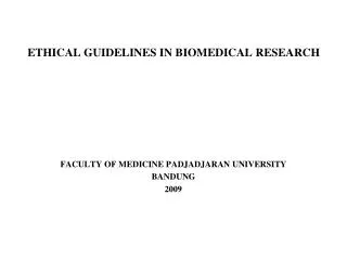
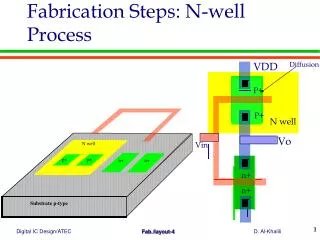
Fabrication Steps: N-well Process
VDD. Fabrication Steps: N-well Process. Diffusion. P+. P+. N well. Vo. Vin. N well. p+. p+ p+. p+. n+ n+. n+. n+. Substrate p-type. Fabrication Steps: N-well Process. VDD. Diffusion. P+. P+. N well. Vin. Vo. N well. p+.

Fabrication Steps: N-well Process
E N D
Presentation Transcript
VDD Fabrication Steps: N-well Process Diffusion P+ P+ N well Vo Vin N well p+ p+ p+ p+ n+ n+ n+ n+ Substrate p-type
Fabrication Steps: N-well Process VDD Diffusion P+ P+ N well Vin Vo N well p+ p+ p+ p+ n+ n+ n+ n+ Substrate p-type
Fabrication Steps p+ p+ n+ n+ N well p+ p+ n+ n+ N well Substrate P-type
Fabrication Steps Oxidation oxide Substrate p-type Patterning of N-well mask Substrate p-type
Fabrication Steps Diffusion: N dopant, Removal of Oxide N-well Si3N4 Deposit Silicon Nitride N-well
Fabrication Steps Patterning: Diffusion (active) mask N-well substrate FOX FOX FOX Oxidation substrate
Fabrication Steps Thin oxide FOX FOX FOX Remove Si3N4 Grow thin oxide N-well Deposit polysilicon N-well
Fabrication Steps Patterning of Polysilicon Poly gates FOX FOX FOX N -well substrate
Fabrication Steps p+ layer P+ Layers and n+ Layer in the Layout polysilicon N well n+ layer
Fabrication Steps Formation of n+ and p+ Diffusion Areas: P+ Diffusion: - Covering with photo-resist - Patterning of the n+ layer - Diffusion: n+ dopant PR FOX FOX FOX N-well p+ dopant
Fabrication Steps Formation of n+ and p+ Diffusion Areas: N+ Diffusion: - Cover with photo-resist - Patterning of the n+ layer - Diffusion: n+ dopant PR p+ p+ N-well n+ dopant p+ p+ n+ n+ N-well
Fabrication Steps p+ layer polysilicon metal P well n+ layer contact
Fabrication Steps SiO2 Strip PR and Deposit Oxide FOX FOX FOX N-well Substrate Patterning of Contact Mask contact p+ p+ n+ n+ N-well Substrate
Fabrication Steps Deposit metal layer Patterning of metal layer Passivation FOX FOX N-well Substrate Deposit Passivation layer
CMOS: 3D Structure p+ p+ FOX FOX n+ n+ FOX N-well Substrate (P-type)
VDD S G B MP D Vin Vout D G B MN S GND The Bulk Contacts VDD n+ layer p+ layer polysilicon metal N-Well N well n+ layer (substrate) contact p+ layer Note: Butting contacts provide more efficient area utilization GND
N-Well CMOS n+ layer p+ layer metal n+ layer contact p+ layer P-well
Twin Tub/Double Layer Metal CMOS Passivation metal II Via Via SiO2 Metal I Metal II FOX n-wel l p-well Substrate P well
Layout Design Rules • Specifies geometrical constrains on the layout art work • Dictated by electrical and reliability constraints with the capability of fabrication technology • Addresses two issues: • reproduction of features on silicon • interaction between layers • Main approaches to describe rules: • based (scalability) • absolute width spacing overlap extension spacing
Based CMOS Design Rules : N Well Process A. N-well A.1 Minimum size 10 A.2 Minimum spacing 6 (Same potential) A.3 Minimum spacing 8 (Different potentials) B. Active (Diffusion) B.1 Minimum size 3 B.2 Minimum spacing 3 B.3 N-well overlap of p+ 5 B.4 N-well overlap of n+ 3 B.5 N-well space to n+ 5 B.6 N-well space to p+ 3 B3=5 n+ B4=3 p+ B5=5 n+ N-well B6=3 B1=3 p+ p+ B2=3
Based CMOS Design Rules C3=1 C PolyI C.1 Minimum size 2 C.2 Minimum spacing 2 C.3. Spacing to Active 1 C.4. Gate extension 2 D. p-plus/n-plus D.1 Minimum overlap of Active 2 D.2 Minimum size 7 D.3 Minimum overlap of Active 1 in abutting contact D.4. Spacing of p-plus/n-plus to 3 n+/p+ gate C4=2 C2=2 C1=2 D2=7 D2=7 active active p-plus n-plus D1=2
Based CMOS Design Rules E4=2 E3=2 E. Contact E.1 Minimum size 2 E.2 Minimum spacing (Poly) 2 E.3 Minimum spacing (Active) 2 E.4 Minimum overlap Active) 2 E.5 Minimum overlap of Poly 2 E.6 Minimum overlap of Metal 1 E.7 Minimum spacing to Gate 2 F. Metal 1 F.1 Minimum size 3 F.2 Minimum spacing 3 G. Via G.1 Minimum size 3 G.2 Minimum spacing 3 G.3 Minimum Metal I overlap 1 G.4 Minimum Metal II overlap 1 E1=2 F2=3 E6=1 F1=3 Metal I E5=2 H1=3 Metal II G2=3 H2=4 G3,G4=1
Based CMOS Design Rules H. Metal II H.1 Minimum size 3 H.2 Minimum spacing 4 I. Via2 I.1 Minimum size 2 I.2. Minimum spacing 3 J. Metal III J.1 Minimum size 8 J.2. Minimum spacing 5 J.3 Minimum Metal II overlap 2 K. Passivation K.1 Minimum opening 100m K.2 Minimum spacing 150m
Layout of a CMOS Inverter Based Design Rules N-well C1 B3 p-plus B4 n-plus E6 Active Via Metal II G1 p-plus n-plus E4 D1 metalI C4
Stick Diagram Notation • It helps to visualize the function as well as topology • It helps in floor planning • 4 layers for SLM: Poly, diffusion, metal, contact • 6 layers for DLM: Poly, Diffusion, Metal I, Metal II, Contact, Via • Construction Guidelines: • When two wires of the same color intersects or touch, they are electrically connected. • Contacts represented by (X) and via by ( ) • When poly crosses diffusion, a transistor is formed • PMOS transistors identified by a small circle around the poly-diffusion intersection
VDD S G B MP D Vin Vout D G B MN S GND Stick Diagram Notation VDD Vout Vin GND
Mixed Notation C B A C
Standard Cells • Modularized approach for layout • Follows certain guidelines in designing these modules • Each module represents a basic combinational or sequential logic function. • Each module has a standard height and variable width referred to as Standard Cell • A collection of these cells referred to as a Standard Cell Library • ASIC Designers deal with abstracted representation of these cells to construct a complete design • The abstracted representation is referred to as the Foot Print • Each abstracted representation consists of input and output terminals referred to as I/O Ports Foot Print Cell Name I/O ports
Standard Cells Output port Input port
VDD INV OUTPUT INPUT VSS Standard Cells Output Port Input Port
Standard Cells For DLM process, vertical routes use metal II. Horizontal routes use Metal I Notice the connections between Metal I and Metal II For Multi-level metal processes cell rows are flipped and butted. Routing can be made on top of the cell rows Routing Channel (More to come in section 5)
Yield Analysis Yield is defined as : Number of Good chips on waferX 100% Total Number of chips Influenced by Defect density Chip area Design rule lithography dimensions Number of mask levels Defects Crystal defects film deposition and growth defects photo-resist imperfections
Yield Analysis Models: 1. Seed’s model for large chips and low yields A= chip area D= defect density 2. Murphy’s model for small chips and high yields