In Technology Size Does Matter
In Technology Size Does Matter. In the world of Microchip design and fabrication the industry is constantly pushing for smaller, more viable structures. Bradley Smrstick Physics Teacher TBT HS 2003. In Technology the Atom is big.

In Technology Size Does Matter
E N D
Presentation Transcript
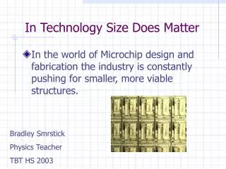
In Technology Size Does Matter • In the world of Microchip design and fabrication the industry is constantly pushing for smaller, more viable structures. Bradley Smrstick Physics Teacher TBT HS 2003
In Technology the Atom is big. • They are fast approaching atomic sized structures where silicon is the pallet, thin film growth is the process and the atom is the paint.
When smaller is better. • Scientists at the University of Illinois have developed a way to produce microscopic pipes capable of transporting fluids in a 3D lattice structure on the order of 10-6 meters.
Applications in Technology • R&D Magazine reports significant implementation of this technology taking place at; IBM Infineon Technologies MetriGenix & Affymetrix BioRad Laboratories University of Illinois
In the beginning... • All microchips share the same origin. • pure • clean • silicon • wafer.
The Processes... • There are actually many different processes used to create a layer. • Each method has its pros & cons. • The two major methods used are • Thin film deposition • Thin film growth
The deposition process... • Thin film deposition involves a process whereby a layer (thin film) is actually deposited on the surface of the silicon.
The growth process... • Thin film growth involves a process whereby a layer (thin film) is actually grown on the surface of the silicon.
Both processes ... • This will likely involve a combination of many processes including • chemical • physical • thermodynamic
From start to finish • In the image to the right a wafer is shown in three states. • Oxidized • Bare • Complete
The Transistor • It takes as many as 300-400 steps to make a Pentium (CMOS)!
Exit to the Masking Process • This process is repeated to generate as many masks as are necessary to complete the microchip in advance of the production phase. • They are then saved and loaded into an automated device that will properly place and change the masks where necessary in the process.
Return from the Masking Process • Continue the process...
That is only one cycle... • This process repeats many times...
Return for the Next Dielectric Deposition • This cycle continues until...
The patterning is complete. • It is time to exit this part of the cycle...
Metrology and Inspection • Scanning Electron Microscopes (SEM)
Metrology and Inspection • Many computer aided inspections are necessary
What is next? • How can we use this chip?
I) We begin a second cycle... • The Copper Interconnect Cycle
Is the Process complete? • If not continue to step I...
I) Continue with the deposition • This may continue many times...
When the process is finally complete? • Exit the Copper Interconnect Cycle
Applications in Technology • These and other related technologies are being implemented in toady's high technology laboratories today according to R&D Magazine as recently as in the April and May issues from 2003.
Innovation is Key • At IBM the introduction of truly NEW Technologies is a high priority. • This lead to the inception of thin polymer films with applications including LCD enhancement, polarizers and reflectors to improve monitor performance characteristics
Saving time is essential. • At MetriGenix a Flow-Thru biochip system has been developed that allows researchers to simultaneously analyze the reaction of up to 400 known genes to a specific substance.
Saving time is essential. • Using the 4D Array from MetriGenix the scientists at Affymetrix have developed a Gene Chip Scanner that has succeeded in reducing the processing time by a factor of six while requiring significantly less sample and reagent volumes.