Understanding the MOS Capacitor: Accumulation, Depletion, and Inversion Phases in p-type Silicon
This lecture focuses on the behavior of the MOS capacitor with a p-type silicon substrate, detailing the processes of accumulation, depletion, and inversion. It emphasizes key voltage parameters, including threshold voltage (VT), and examines charge density dynamics at the silicon surface. Using Gauss’s Law and Poisson's equation, the relationships between gate voltage, charge distribution, and surface potential are derived. The lecture also discusses the significance of the inversion layer and its impact on charge density, providing essential insights for semiconductor device fundamentals.

Understanding the MOS Capacitor: Accumulation, Depletion, and Inversion Phases in p-type Silicon
E N D
Presentation Transcript
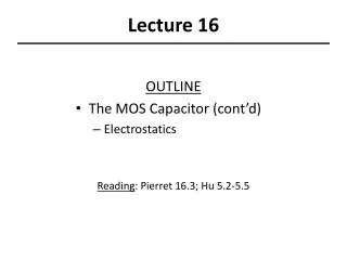
Lecture 16 OUTLINE • The MOS Capacitor (cont’d) • Electrostatics Reading: Pierret 16.3; Hu 5.2-5.5
+ + + + + + - - - - - - Accumulation (n+ poly-Si gate, p-type Si) M O S VG < VFB 3.1 eV | qVox | Ec= EFM GATE Ev |qVG | xo |qfS| is small, 0 + VG Ec _ p-type Si 4.8 eV EFS Ev Mobile carriers (holes) accumulate at Si surface EE130/230A Fall 2013 Lecture 16, Slide 2
+ + + + + + - - - - - - Accumulation Layer Charge Density VG < VFB From Gauss’ Law: GATE xo + VG _ Qacc (C/cm2) p-type Si (units: F/cm2) EE130/230A Fall 2013 Lecture 16, Slide 3
+ + + + + + - - - - - - Depletion (n+ poly-Si gate, p-type Si) M O S VT > VG > VFB qVox W Ec GATE EFS qfS 3.1 eV Ev qVG + VG _ Ec= EFM p-type Si Ev 4.8 eV Si surface is depleted of mobile carriers (holes) => Surface charge is due to ionized dopants (acceptors) EE130/230A Fall 2013 Lecture 16, Slide 4
Depletion Width W (p-type Si) • Depletion Approximation: The surface of the Si is depleted of mobile carriers to a depth W. • The charge density within the depletion region is • Poisson’s equation: • Integrate twice, to obtain fS: To find fs for a given VG, we need to consider the voltage drops in the MOS system… EE130/230A Fall 2013 Lecture 16, Slide 5
+ + + + + + - - - - - - Voltage Drops in Depletion (p-type Si) From Gauss’ Law: GATE + VG _ Qdep (C/cm2) Qdep is the integrated charge density in the Si: p-type Si EE130/230A Fall 2013 Lecture 16, Slide 6
Surface Potential in Depletion (p-type Si) • Solving for fS, we have EE130/230A Fall 2013 Lecture 16, Slide 7
Threshold Condition (VG = VT) • When VG is increased to the point where fs reaches 2fF, the surface is said to be strongly inverted. This is the threshold condition. VG = VT • (The surface is n-type to the same degree as the bulk is p-type.) EE130/230A Fall 2013 Lecture 16, Slide 8
MOS Band Diagram at Threshold (p-type Si) M O S qVox WT qfF Ec EFS qfF qfs Ev qVG Ec= EFM Ev EE130/230A Fall 2013 Lecture 16, Slide 9
Threshold Voltage • For n-type Si: • For p-type Si: C. C. Hu, Modern Semiconductor Devices for ICs, Figure 5-8 EE130/230A Fall 2013 Lecture 16, Slide 10
+ + + + + + - - - - - - Strong Inversion (p-type Si) As VG is increased above VT, the negative charge in the Si is increased by adding mobile electrons (rather than by depleting the Si more deeply), so the depletion width remains ~constant at W = WT WT r(x) M O S GATE x + VG _ p-type Si Significant density of mobile electrons at surface (surface is n-type) EE130/230A Fall 2013 Lecture 16, Slide 11 R. F. Pierret, Semiconductor Device Fundamentals, p. 575
Inversion Layer Charge Density (p-type Si) EE130/230A Fall 2013 Lecture 16, Slide 12
fS and W vs. VG(p-type Si) 2fF fS: 0 VG accumulation depletion inversion VFB VT W: 0 VG accumulation depletion inversion VFB VT EE130/230A Fall 2013 Lecture 16, Slide 13
Total Charge Density in Si, Qs(p-type Si) depletion inversion 0 VG accumulation VFB VT accumulation depletion inversion accumulation depletion inversion VG 0 VFB VT VG 0 VFB VT accumulation depletion inversion VG 0 Qinv VFB VT slope = -Cox EE130/230A Fall 2013 Lecture 16, Slide 14

