Sensor Signal Conditioning in Electronic Instruments
890 likes | 1.48k Vues
Learn about different circuit schematics for signal conditioning between sensors and instruments, covering types, amplification, isolation, and more. Explore the evolution and parameters of operational amplifiers in electronics engineering.

Sensor Signal Conditioning in Electronic Instruments
E N D
Presentation Transcript
SENSORSIGNAL CONDITIONING INSTRUMENTATION ENGINEERING EE531 AMU
Electronic Instrument. Block Diagram. Physical Variable Electrical Signal M S Indicating Element Electronic Processor SENSOR ? Analog meter.DigitalDisplay(numeric, alphanumeric, graphic) Electronic Circuit analog or digital IC.(Opamps, glue logic,microprocessor), instrument,PC
V Example 1 • Thermocouples. When we connected two different wires of specific materials , an emf appears in its terminals that dependents on T2, T1 and the materials A, B. This emf is a low value signal , typically millivolts, to detected properly we need to amplify. We can’t connect directly into an instrument (voltmeter or ADC). When we connected two different wires of specific materials , an emf appears in its terminals that dependents on T2, T1 and the materials A, B. This emf is a low value signal , typically millivolts, to detected properly we need to amplify. We can’t connect directly into an instrument (voltmeter or ADC). SIGNAL CONDITIONING IS NEEDED !!!
V Example 2 • A forward bias diode has a linear variation with temperature but with a negative slope. • To avoid self heating effects I should be minimized around some micro- Amperes. • We can’t connect it directly in some instrument. We need a positive slope and evaluate the loading effect. SIGNAL CONDITIONING IS NEEDED !!! SIGNAL CONDITIONING IS NEEDED !!! SIGNAL CONDITIONING IS NEEDED !!!
OBJECTIVE • Characterize different circuit schematics available to signal conditioning between sensor signals and instruments. S M TRANSDUCER SIGNAL CONDITIONING INSTRUMENT S=f(M) ?
Lect 4. SENSOR SIGNAL CONDITIONING Outline: • Introduction • Analog ICs. • Signal Conditioning Types. • Amplification. • Isolation. • Impedance Matching. • Wheastone Bridges. • V/V, I/V , V/I Converters. • V-f, f-V Converters • Filters • Digital Converters. • Others.
REFERENCES • Sensor Technology Handbook. Jon Wilson. Cap4. pag(31-108).Elsevier 2005 • Practical Data Adquisition for Instrumentation and Control Sistem. John Park, Steve MacKay. Cap 3. pag(33-66). Elsevier. 2003. • Process Control Instrumentation Technology. Curtis D. Johnson. Cap 2 y 3. Prentice Hall. 2000.
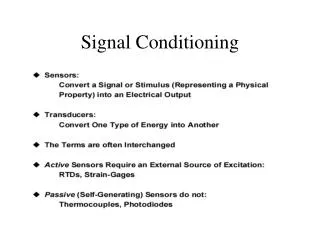
Integrated Circuit Survey • Operational Amplifiers. • Instrumentation Amplifiers. • Isolation Amplifiers. • Frequency Converters. • ADC & DAC .
OPAMP • Basic component of Analog Electronics. (Work horse!!!) • A wide range of OPAMPS are commercially available to fulfill design requirements of many applications. • Others IC are built by integrating Schematics with several OPAMPS. (active filters, Instrumentation Amplifier).
OPAMP • Basic parameters. • Differential inputs with high impedance. • Low output impedance • High open loop Gain • Single – Double Power Supply • Bandwidth from DC.
REAL OPAMPS • Input offset voltage: when inputs are connected to ground output is not zero. There is a small difference between inputs. • 0ffset current: offset voltage is really produced by a difference in input current. • Input bias current: is the mean of input currents in order to make the output zero. • Slew rate: if the input changes with time as a step function , the output goes to saturation voltage. However the output needs a time to go into saturation. Slew rate is characterized by the slope of output voltage with time [ V/us]. • Unity gain frecuency bandwith: the frequency when differential gain is one. • Common Mode Rejection Ratio CMRR: output is a function of the differential input ( differential gain Ad ) but also is a function of the common voltage at the output (common gain Acm). CMRR is the ratio of Ad/Acm
More parameters • Power supply rejection ratio PSRR: When PS change, the output voltage should be the same. However in practice there is some changes. This parameter takes account this effect. Is defined as the ratio of changes in PS over changes in output, in dB. It is a function of frequency operation.
Input offset voltage • A main source of systematic error in OPAMPS. • Input offset compensation is getting by hardware, by software or by technology.. • Input offset voltage also has a drift with time and temperature.
How are OPAMP Technologies evolved. uA741 !!!
2. INSTRUMENTATION AMPLIFIER: In-Amp Its is improved version of differential amplifier.
Three OPAMPs Instrumentation Amplifier: In-Amp. Assuming that R2=R3, and R4=R5=R6= R7 equals
Basic In-Amp. • High balanced input impedance. • Differential gain is set up by a external resistor value Rg. • High CMRR typically of 80-100dB
Instrumentation Amplifier : Typical Application. • Wheastone Bridge Signal Conditioning. • Small floating differential signal is transformed into a single signal (reference to ground) , with low output impedance and some gain. • The high input impedance guaranties low loading effect.
3. Isolation Amplifier :ISO-Amps • Isolated systems: There are many applications where it is desirable, or even essential, for a sensor to have no direct (“galvanic”) electrical connection with the system to which it is supplying data. • To avoid the possibility of dangerous voltages or currents from one half of the system doing damage in the other. • Such a system is said to be “isolated,” and the arrangement which passes a signal without galvanic connections is known as an “isolation barrier.” • The isolation amplifier has an input circuit that is galvanically isolated from the power supply and the output circuit. In addition, there is minimal capacitance between the input and the rest of the device. Therefore, there is no possibility for DC current flow, • Industrial Measurements: Monitoring Motors. • Biomedicine :ECG, EEG, EMG . • Objective : to provide a barrier in both sense.
Application: current sensing in Motors. 440 V INSTRUMENT
4. High Impedance Sensor Coupling Techniques. Many popular sensors have output impedances greater than several MΩ, and the associated signal conditioning circuitry must be carefully designed to meet the challenges of low bias current, low noise, and highgain.
IV Converter • Photodiodes may either be operated with zero bias (photovoltaic mode, left) or reverse bias (photoconductive mode, right) • Photodiode current is converted to Voltage when it flows through feedback resistor of OPAMP. • To measure 30pA we get 30 mV with a feedback resistor of 1000 Mohms. • Notice that we have chosen to get as much gain as possible from one stage, rather than cascading two stages. This is in order to maximize the signal-to-noise ratio (SNR). • To accurately measure photodiode currents in the tens of picoamps range, the bias current of the op amp should be no more than a few picoamps. This narrows the choice considerably.
OPAMP selection • The industry-standard OP07 is an ultra-low offset voltage (10μV) bipolar op amp, but its bias current is 4 nA (4000 pA!). • A FET-input electrometer-grade op amp is chosen for our photodiode preamp, since it must operate only over a limited temperature range.(FETs currents double every 10ºC!!.
PH sensor Signal Conditioning. A typical pH probe requires a buffer amplifier to isolate its 10^6 to 10^9 Ω source resistance from external circuitry. The low input current of the AD795 allows the voltage error produced by the bias current and electrode resistance to be minimal.
Thevenin Equivalent of PH Sensor Rth=100M ?
5-Filters • There is a need to remove or attenuate undesired signals that are presented in sensor circuits. • We can use active of passive filters. Active filters provide more abrupt transitions and better stability.