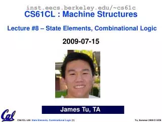
James Tu, TA
inst.eecs.berkeley.edu/~cs61c CS61CL : Machine Structures Lecture #8 – State Elements, Combinational Logic 2009-07-15. James Tu, TA. What are “Machine Structures”?. Coordination of many levels of abstraction. 61C. Application (Netscape). Operating. Compiler. System (MacOS X).

James Tu, TA
E N D
Presentation Transcript
inst.eecs.berkeley.edu/~cs61cCS61CL : Machine StructuresLecture #8 – State Elements, Combinational Logic2009-07-15 James Tu, TA
What are “Machine Structures”? Coordination of many levels of abstraction 61C Application (Netscape) Operating Compiler System (MacOS X) Software Assembler Instruction Set Architecture Hardware Processor Memory I/O system Datapath & Control Digital Design Circuit Design transistors ISA is an important abstraction level:contract between HW & SW
61C Levels of Representation temp = v[k]; v[k] = v[k+1]; v[k+1] = temp; lw $t0, 0($2) lw $t1, 4($2) sw $t1, 0($2) sw $t0, 4($2) High Level Language Program (e.g., C) Compiler Assembly Language Program (e.g.,MIPS) Assembler 0000 1001 1100 0110 1010 1111 0101 1000 1010 1111 0101 1000 0000 1001 1100 0110 1100 0110 1010 1111 0101 1000 0000 1001 0101 1000 0000 1001 1100 0110 1010 1111 Machine Language Program (MIPS) Machine Interpretation Hardware Architecture Description (Logic, Logisim, etc.) Architecture Implementation Logic Circuit Description (Logisim, etc.)
Synchronous Digital Systems Synchronous: Means all operations are coordinated by a central clock. It keeps the “heartbeat” of the system! Digital: Mean all values are represented by discrete values Electrical signals are treated as 1’s and 0’s and grouped together to form words. The hardware of a processor, such as the MIPS, is an example of a Synchronous Digital System
Logic Design Next 2 weeks: we’ll study how a modern processor is built; starting with basic elements as building blocks. Why study hardware design? Understand capabilities and limitations of hardware in general and processors in particular. What processors can do fast and what they can’t do fast (avoid slow things if you want your code to run fast!) Background for more detailed hardware courses (CS 150, CS 152, EE 192) There is just so much you can do with processors. At some point you may need to design your own custom hardware.
Signals and Waveforms: Clocks • Signals • When digital is only treated as 1 or 0 • Is transmitted over wires continuously • Transmission is effectively instant • Implies that any wire only contains 1 value at a time
Signals and Waveforms: Circuit Delay 2 3 4 5 3 4 5 6 7 11 5 9
Type of Circuits Synchronous Digital Systems are made up of two basic types of circuits: Combinational Logic (CL) circuits Our previous adder circuit is an example. Output is a function of the inputs only. Similar to a pure function in mathematics, y = f(x). (No way to store information from one invocation to the next. No side effects) State Elements: circuits that store information.
Uses for State Elements As a place to store values for some indeterminate amount of time: Register files (like $1-$31 on the MIPS) Memory (caches, and main memory) Help control the flow of information between combinational logic blocks. State elements are used to hold up the movement of information at the inputs to combinational logic blocks and allow for orderly passage.
Accumulator Example Why do we need to control the flow of information? Want: S=0; for (i=0;i<n;i++) S = S + Xi Assume: • Each X value is applied in succession, one per cycle. • After n cycles the sum is present on S.
First try…Does this work? Feedback Nope! Reason #1… What is there to control thenext iteration of the ‘for’ loop? Reason #2… How do we say: ‘S=0’?
Second try…How about this? Roughtiming… Register is used to hold up the transfer of data to adder.
Register Details…What’s inside? n instances of a “Flip-Flop” Flip-flop name because the output flips and flops between and 0,1 D is “data”, Q is “output” Also called “d-type Flip-Flop”
What’s the timing of a Flip-flop? (1/2) Edge-triggered d-type flip-flop This one is “positive edge-triggered” “On the rising edge of the clock, the input d is sampled and transferred to the output. At all other times, the input d is ignored.” Example waveforms:
What’s the timing of a Flip-flop? (2/2) Edge-triggered d-type flip-flop This one is “positive edge-triggered” “On the rising edge of the clock, the input d is sampled and transferred to the output. At all other times, the input d is ignored.” Example waveforms (more detail):
Recap of Timing Terms Clock (CLK) - steady square wave that synchronizes system Setup Time - when the input must be stable before the rising edge of the CLK Hold Time - when the input must be stable after the rising edge of the CLK “CLK-to-Q” Delay - how long it takes the output to change, measured from the rising edge Flip-flop - one bit of state that samples every rising edge of the CLK Register - several bits of state that samples on rising edge of CLK or on LOAD
Finite State Machines (FSM) Introduction • You have seen FSMs in other classes. • Same basic idea. • The function can be represented with a “state transition diagram”. • With combinational logic and registers, any FSM can be implemented in hardware.
Finite State Machine Example: 3 ones… FSM to detect the occurrence of 3 consecutive 1’s in the input. Draw the FSM… Assume state transitions are controlled by the clock: on each clock cycle the machine checks the inputs and moves to a new state and produces a new output…
Hardware Implementation of FSM … Therefore a register is needed to hold the a representation of which state the machine is in. Use a unique bit pattern for each state. + ? = Combinational logic circuit is used to implement a function maps from present state and input to next state and output.
Hardware for FSM: Combinational Logic PS Input NS Output 00 0 00 0 00 1 01 0 01 0 00 0 01 1 10 0 10 0 00 0 10 1 00 1 Later in today’s lecture, we will discuss the detailed implementation, but for now can look at its functional specification, truth table form. Truth table…
Maximum Clock Frequency What is the maximum frequency of this circuit? Hint… Frequency = 1/Period Max Delay =Setup Time + CLK-to-Q Delay + CL Delay
General Model for Synchronous Systems • Collection of CL blocks separated by registers. • Registers may be back-to-back and CL blocks may be back-to-back. • Feedback is optional. • Clock signal(s) connects only to clock input of registers. (NEVER put it through a gate)
Administrivia • Project 2 due Friday @ 11:59 PM • Midterm 7/20 (Monday) in class
Combinational Logic FSMs had states and transitions How to we get from one state to the next? Answer: Combinational Logic
And vs. Or review – Dan’s mnemonic Symbol Definition A C B AND Gate AND
2-input gates extend to n-inputs N-input XOR is the only one which isn’t so obvious It’s simple: XOR is a 1 iff the # of 1s at its input is odd
Boolean Algebra George Boole, 19th Century mathematician Developed a mathematical system (algebra) involving logic later known as “Boolean Algebra” Primitive functions: AND, OR and NOT The power of BA is there’s a one-to-one correspondence between circuits made up of AND, OR and NOT gates and equations in BA + means OR,• means AND, x means NOT
Boolean Algebra (e.g., for majority fun.) y = a • b + a • c + b • c y = ab + ac + bc
BA: Circuit & Algebraic Simplification BA also great for circuit verificationCirc X = Circ Y?use BA to prove!
Canonical forms (1/2) Sum-of-products (ORs of ANDs)
Review Use this table and techniques we learned to transform from 1 to another
N instances of 1-bit-wide mux How many rows in TT?
4-to-1 Multiplexor? How many rows in TT?
Is there any other way to do it? Hint: March Madness Ans: Hierarchically!
_B A NOR P 0 A NOR NOR C 0 B’ B 0 D C Q 1 1 0 0 P 1 Q A D Do you really understand NORs? • If one input is 1, what is a NOR? • If one input is 0, what is a NOR? A B NOR 0 0 1 0 1 0 1 0 0 1 1 0
A NAND B 1 A P NAND 0 NAND _B C 0 1 D C Q 1 1 B’ 0 P 1 Q A D Do you really understand NANDs? • If one input is 1, what is a NAND? • If one input is 0, what is a NAND? A B NAND 0 0 1 0 1 1 1 0 1 1 1 0


