Download
1 / 23
270 likes | 700 Vues
Nanoscale Defects in Graphene . Andrew Evans, Justin Matson, Mohannad Bukhamseen , Wakaas Shafi . papers: - Spatial control of defect creation in graphene at the nanoscale - Nanoparticle structures served up on a tray (Billinge 453-54). Graphene - What is it?.

E N D
Nanoscale Defects in Graphene Andrew Evans, Justin Matson, Mohannad Bukhamseen , Wakaas Shafi papers: - Spatial control of defect creation in graphene at the nanoscale - Nanoparticle structures served up on a tray (Billinge 453-54)
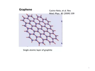
Graphene - What is it? • Substance composed of pure carbon, with atoms arranged in a regular hexagonal pattern similar to graphite, but in a one-atom thick sheet. It is very light, with a 1-square-meter sheet weighing only 0.77 milligrams. Picture Credit: AlexanderUIS Graphene is an atomic-scale honeycomb lattice made of carbon atoms. Picture Credit: AlexanderUIS Carbon atom, credit: protondecay.blogspot.com
Defect Creation in Graphene • Why create defects in graphene? • Defects in graphene alter: 1) electrical properties 2) chemical properties 3) magnetic properties 4) mechanical properties Defect in Graphene Credit: http://nextbigfuture.com/2010/11/graphene-produced-with-controlled.html Defects
Defect Creation in Graphene • Why create defects? • We can intentionally make use of its altered properties • How do we create defects? • Ion irradiation can induce atomic defects in graphene. Ion irradiation facility Credit: http://www.dreebit.com/en/products/ion_irradiation_facility_m_31/
Objectives Vacancies in a sheet of Graphene (orange) are filled with Iridium atoms (blue). • Describe a method to control defects in a sheet of Graphene. • Dope a sheet of graphene with a material that is used as a catalyst, such as an Iridium substrate. • Lay the Iridium atoms on the sheet.Study the structure and the arrangement of the Iridium nanoparticles. Iridium(111) Graphene When Iridium is placed on the doped sheet, it is arranged in a specific pattern and structure. Nature Materials9,291–292 (2010 )doi:10.1038/nmat2733
Catalysis • What we know: • Catalysts reduce the rate of a reaction by providing a surface of nanoparticles for the reagents to react on. • The atoms at the surface of the catalyst rearrange to increase the surface area and decrease the surface energy. This changes the reactivity and the interactions between the reagents. • The catalyst is not consumed during the process. • What we don't know: • How the nanoparticles at the surface are arranged. • What the surface structure looks. Molecule bonding on a catalyst foundation Nature430, 730 (12 August 2004) | doi:10.1038/430730a; Published online 11 August 2004
Importance of Catalysts • Basis for "20-30% of the GNP" (Gross National Product) • Used Everywhere: • Processing of fuels • fertilizers • polymers • pharmaceuticals • energy • Need for new catalysts for energy conversion http://www.rita.dot.gov/bts/sites/rita.dot.gov.bts/files/publications/the_changing_face_of_transportation/images/figure_01_us_gross_national_product.gif Catalysts lower activation energy for reactions. Credit: ch302.cm.utexas.edu * Maxwell, Stud. Surf. Sci. Catal. 101, 1 (1996)
The Challenge: To develop a molecular level picture of the way surfaces catalyze chemical transformations. To use these images to understand how the nanoparticles are arranged on the surface of the catalysts. To understand how do the nanoparticle's arrangement translate to a lower activation energy during reactions? To use this insight to produce and design new catalysts for better energy conversion. Separate molecules react while bonded to the catalyst foundation.
Possibilities for Catalysis Possibilities for Society Enabling nanoscale catalysts Resources Energy Chemical Production In this transmission electron micrograph of the mesoporous nanospheres, the nano-scale catalyst particles show up as the dark spots. Using particles this small (~ 3nm) increases the overall surface area of the catalyst by roughly 100 times. http://www.thebioenergysite.com/news/contents/08-08-14Nano.jpg . Environmental Protection
Graphene and Catalysis • It was shown that the binding and molecular absorption of Pt nanoparticles onto a sheet of graphene can be controlled by inducing defects on graphene • By doping the graphene sheet with nitrogen the Pt nanoparticles can tolerate CO more when the particles are deposited on the nitrogen induced graphene sheet • Creating defects that can affect the binding and absorption of nanoparticles on graphene, can help us design a construct new and more efficient catalysts for our everyday chemical processes Image above shows catalytic performance, particularly tolerance against CO poisoning and particle migration, of Pt nanoparticles dispersed on graphene using ab initio calculations. http://pubs.acs.org/appl/literatum/publisher/achs/journals/content/ancac3/2011/ancac3.2011.5.issue-2/nn1017395/production/images/medium/nn-2010-017395_0006.gif http://cdn.physorg.com/newman/gfx/news/hires/graphenecatalyst.jpg
Surface Geometry • Catalytic efficiency is highly dependent on surface geometry • Understanding that geometry can inform efficient catalyst production • Analyzing surface geometry on nanoscale catalysts is extremely difficult A catalyst in action with a highly ordered surface geometry Example of a nanocatalyst: Credit: research.che.tamu.edu -
Issues to address • The surface atoms can be studied with the use of synchrotron X-ray sources. However, the atoms can only be seen if they are arranged in a periodic manner. • Note that an alternate solution would be developing more sophisticated methods for observing nanoscale geometries • To be able to study the atoms, we need to have a surface that will allow the catalyst atoms to be arranged periodically. http://media.wiley.com/Lux/52/287752.image0.jpg Periodic layers and moire pattern. Credit:http://iopscience.iop.org/0953-8984/24/31/314210/article
Defect Creation in Graphene • Ion radiation is not the best method to induce defects because the defects are randomly scattered over large distances. • We need more accuracy, so we look to: exposing graphene to an electron beam. http://www.nature.com/ncomms/journal/v3/n10/images/ncomms2141-f1.jpg Broad beam (no defects) Focused beam Broad beam (with defects)
Defects in Graphene The knock-on damage threshold of Graphene is 86 KeV. Subjecting a monolayered sheet of Graphene to an electron beam irradiation with a potential higher than that will form defects. Reports show that setting the electron beam irradiation potential to 80 KeV, while varying the beam current density (BCD) and the exposure time, can make the process of creating defects inGraphene controllable, and confined to an area of 10X10 nm^2 It was found that when the sheet is exposed to a (BCD) of ~10^8 e−1 nm−2 s−1 for 30 seconds a divacancy was created. Images of three different 30 s exposures, resulting in: (c) a divacancy.(d) a divacancy having undergone a single stone-Wales bond rotation and (e) two linked divacancies along the armchair direction. a) AC-TEM image of a pristine graphene sheet before 30 s exposure to a focused electron beam. b) Divacancy formed in exposure area directly after irradiation. Nat. Commun. 3:1144 doi: 10.1038/ncomms2141 (2012).
Images of defects formed after 60s of focussed electron beam irradiation: a) Three linked divacancies. b) A divacancy after a SW transformation. c) Defects clustered around one of a pair of dislocations. [Nat. Commun. 3:1144 doi: 10.1038/ncomms2141 (2012) ] Images of defects formed after 120 s of focussed electron beam irradiation:g) An enclosed, rotationally misaligned core of six hexagons, surrounded by a complete loop of pentagons and heptagons. h) A larger, partially completed loop, isolating several rotated hexagons. A gap in the loop, filled by two hexagonal rings, is highlighted in red. The arrow marks an adatom, which inhibits direct interpretation of the area bordered in black due to localized lattice distortion arising from the adatom. i) Two divacancy defects, each having been transformed via two sW rotations, leading to a single isolated, rotated hexagon.
Exposure Time (sec) Average Atoms Lost (nm^-2) A bar chart parameterizing the effect of exposure time on defect complexity, defined here as the number of non-six-membered carbon rings plus any rotationally mismatched six-membered rings in the irradiated area, parameterized as the NDV. Normalized Defect Value Total Beam Dose (e^-1 nm^-2) • To dope the Graphene sheet with Iridium, 30s exposure is needed. It creates vacancies that are small, and can be kept under control.
3D rendering of a graphene hole imaged on TEAM 0.5 shows that the carbon atoms along the edge assume either a zigzag or an armchair configuration. Click here to view a video: Atom In Action
Creating controlled defects with an electron beam B) A focused probe with a high current density used to form defects. (BCD goes up to~108 e − 1 nm − 2 s − 1) A) A broad beam used to image graphene before defect formation (typical beam current density ~105 e − 1nm − 2 s − 1) C) A broad beam used to image graphene after defect formation. (BCD goes back to ~105 e − 1 nm − 2 s − 1) Robertson, A.W. et al. Spatial control of defect creation in graphene at the nanoscale. Nat. Commun. 3:1144 doi: 10.1038/ncomms2141 (2012).
A Geometric Solution to the nanostructure problem How do we achieve a periodic arrangement that can be observed by synchrotron x-ray sources? A 3-D representation of a doped sheet of Graphene (black layer) with the Iridium atoms (yellow) arranged periodically on top of it. • It was found that layering a sheet of graphene over an iridium substrate formed the perfect base for causing a periodic arrangement in identical 82-atom nanoparticles of iridium • This periodic arrangement (called a "moire arrangement") is observable with existing techniques.
Applications • Once the iridium forms a moire arrangement on the graphene sheet, observation and analysis is possible. • Specifics of the geometry can be observed • Interaction between the particles and the substrate can be analyzed • Understanding how the substrate is structured and how it interacts allows us to make nanoscale improvements to the catalyst. Moire arrangement on a graphene sheet Credit: Johann Coraux Website: http://perso.neel.cnrs.fr/johann.coraux/index_en.html
Conclusion • We can use Iridium catalysts to increase reaction rates. • We can study the structure and arrangement of nanoscale Iridium catalysts using Graphene sheets. • We can make changes to the reactivity and interactions between the reagents. Graphene sheet Endless applications for graphene
Suggested Research • Study of the nanoscale structure in a temporally and spatially resolved way in a complex, heterogeneous system. • How to create defects in a controlled area with variable complexity, opens up the possibility for enhanced engineering of graphene.
References -Billinge, Simon. "Nanoparticle structures served up on a tray." Nature. 28 MAR 2013: 453-54. Web. 14 Apr. 2013. < http://www.nature.com/nature/journal/v495/n7442/full/495453a.html -Robertson, A.W. et al. Spatial control of defect creation in graphene at the nanoscale. Nat. Commun. 3:1144 doi: 10.1038/ncomms2141 (2012)