Digital Switching
Digital Switching. EE8304/TC715N SMU/NTU Lecture Scheduled March 23, 2004 Direct Memory Access (DMA) and Circuit Switching (print slides only, no notes pages). Overview. Modern computers perform Input/Output (I/O) via a specialized hardware module which uses Direct Memory Access (DMA)

Digital Switching
E N D
Presentation Transcript
Digital Switching EE8304/TC715N SMU/NTU Lecture Scheduled March 23, 2004 Direct Memory Access (DMA) and Circuit Switching (print slides only, no notes pages) ©1997-2004 R. Levine
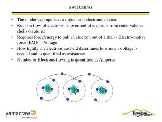
Overview • Modern computers perform Input/Output (I/O) via a specialized hardware module which uses Direct Memory Access (DMA) • It generates a sequence of addresses and autonomously reads/writes RAM memory data, independent of the CPU • The DMA module structure is very similar to a digital switching matrix • With addition of a “Connect Memory” for mapping time sequence of I/O time slots. • Connect memory contains one type of “Translation Table” or “Indirect Address Table” ©1997-2004 R. Levine
Historical Computer I/O • Early computer designs interposed the CPU between the I/O port and the memory • This was slow and inefficient: • Many early I/O devices (keyboard or printer) were much slower to handle a character than the speed of the CPU • Program code involving indefinitely long wait loops was used to cause a read-in of data when a keyboard character was ready, or to print the next output character. Typical input assembly language: BACK: JMPI RIN; {test the “readyinput” signal} JMP BACK; {go back} RIN: READ REG1; {copy input line to register 1} • Invention of interrupt technology improved the I/O process somewhat Note: BACK: and RIN: are assembly language statement line labels. JMPI is a conditional jump that depends on a data ready flag signal from an input channel. ©1997-2004 R. Levine
Deficiencies of CPU I/O • In previous example, no other useful CPU operations can be accomplished while waiting for I/O • Large data block I/O transfers could occupy most of the program run time • known as “I/O bound” or “I/O limited” programs • Early I/O devices were very slow, thus compounding the problem • Example: 10 character/second printer, compared to megabyte/second transfer rates to a VGA computer display today • Keyboard input is still slow today ©1997-2004 R. Levine
Interrupt Improvements • By use of an interrupt process for each input character (or text line), the CPU allows other useful work between character inputs • Particularly helpful in a multi-user computer (“time sharing”) • Each keystroke causes an electrical interrupt signal (for character-oriented input): • Character is stored in a 1-byte external “buffer” register • Interrupt service routine (ISR) reads in the character • Upon completion of the ISR, the computer returns to the original ongoing program code execution • Note: some input systems store a string of characters in a larger buffer, and cause an interrupt only when a particular character (like the ENTER key) is pressed. ©1997-2004 R. Levine
Direct Memory Channel Improvement • Interrupt processing is better than looping while waiting for input, but still requires explicit op-code cycles to perform I/O transfers • Next improvement is a separate peripheral module to perform direct memory access (DMA) • independent channel to/from RAM • Generates its own sequence of address values • Starting address pre-set by CPU • End address (or data block length) pre-set by CPU • Some DMA designs contain a buffer memory • Executes its data transfer cycles without slowdown of the CPU, via “cycle stealing” ©1997-2004 R. Levine
Cycle “Stealing” • Most computer operation op-code cycles have two distinct parts: • One part involves RAM access • Read the OP code from program memory • Read/write data from/to data RAM address(es) • Second part involves only CPU operations • Perform data manipulation using CPU registers as source(s) and destination(s) of data • DMA device performs RAM access during this second portion of the op-code cycle ©1997-2004 R. Levine
DMA Block Diagram Interrupt line cycle state signals CPU DMA Module External I/O lines address setup Address bus Data bus Many devices connect to a bus; control signals (not shown) determine which device is the destination of the current bus data values. DMA has same clock input as CPU. Some designs use main address bus to transfer initial DMA start/stop address settings. RAM ©1997-2004 R. Levine
DMA Module Comprises: • Address Generator • Automatically incrementing/decrementing address register • Starting value is pre-set by CPU • Special full adder module to automatically add/subtracts 1 (or other appropriate value) to address register contents for each RAM access cycle • End Control • End address register • value pre-set by CPU • Comparison hardware • Current DMA access address is compared with contents of end address register after each read/write cycle • Repetitive RAM access and address increment cycle is electrically stopped when all bits match • Then DMA causes a distinct CPU interrupt indicating “I’m finished with the block transfer” ©1997-2004 R. Levine
DMA Conditions • Data is transferred in blocks. Data bytes go to/from consecutive RAM addresses • Special case of 1-byte block is also used • For “continuous” transfer, external device data rate must be sufficiently fast: • Magnetic disk bit transfer is rapid • There is some delay (latency) until proper track/sector is under the read/write magnetic pickup head, but then the bit rate is fast • Data to/from devices with slow or non-regular data byte transfers is typically “buffered” in an external or peripheral memory • Example: keyboard buffer stores characters until special key (e.g., “ENTER”) is pressed • buffer is internal to DMA module in some designs ©1997-2004 R. Levine
DMA Transfer • During DMA data transfer a data word (byte, etc.) is transferred during the appropriate (“stolen”) part of each consecutive op-code cycle • Sometimes called “background” operation • Meanwhile, unrelated CPU “foreground” op-codes may be executed • When block transfer is complete, DMA causes a CPU interrupt • When the total data array is very large, it is typically segmented and transferred in fixed size blocks • In general, transfer block size is arbitrary • In some cases, transfer block size is fixed by external buffer or device constraints • example: 512 bytes in a diskette data block ©1997-2004 R. Levine
DMA Today • Most (except some very simple 4-bit) CPU chips have DMA modules “built in” today1 • Standard “feature” of all personal computers • Most CPUs do not have an INPUT or OUTPUT op-code, but do have op-codes to set up the DMA module to perform I/O • Four commands to: set start address; set end address (or block size); read or write via a particular I/O channel; then start transfer. • Special separate memory with special DMA modules performs digital telecommunications switching as well • standard method for circuit switching • can also be used for cell switching (ATM, fast packet, etc.) although other specialized structures also exist Note 1: We cannot call this built-in DMA a “peripheral” device ©1997-2004 R. Levine
Some History • Telephone systems used “circuit switching” via space switches • A channel is dedicated to the two (or more in a conference call) participants for the duration of the conversation • regardless of whether sound or silence is present at the microphone • historically achieved by analog metallic wire conductor connection of the two telephones • When digital multiplexing (T-1 channel banks) were introduced (ca. 1961), engineers’ thoughts soon turned to fully electronic digital switching • Many historical designs exist for mechanically moving contacts to the correct pair of wires, or closing the selected contacts in relays • Gross-motion switches: contact arms rotate or slide • Step-by-step (Strowger, Automatic Electric*) • X-Y and Radial-angular (Ericsson and Stromberg-Carlson**) • Panel (AT&T***) used in 1930s-1960s • Fine-motion switches: relay armatures pivot with small contact movement • Multi-relay tree switching, code switches, etc. Various developers, mainly for small private branch exchange (PBX) switches. • Crossbar (Ericsson and AT&T***) * Later GTE A.E., now merged into AG Communications Systems; **S-C now merged into Siemens; ***AT&T manufacturing operations are now Lucent (and Avaya PBXs) ©1997-2004 R. Levine
“Electronic” vs. Digital Switching • The first digital switch in the PSTN is generally acknowledged to be the AT&T (now Lucent) No. 4 ESS (electronic switching system), circa 1970 • several earlier switching systems, called electronic, still used electromechanical switching (typically small relays) and analog transmission (example: No. 1 ESS) • 4 ESS is a transit or tandem switch, not a central office or end office • 4 ESS has only T-1 links at its ports (no telephone sets*) • analog/digital conversion and digital multiplexing is done elsewhere in the PSTN by channel banks or digital central offices • The first commercial digital “end” switch (a PBX) is credited by most sources to ROLM** circa 1970. • ROLM was a military computer maker, illustrating that good ideas sometimes come from outside the traditional telecom industry • Original design not internally compatible with 64 kb/s Mu-law PCM *except for some test lines; **later merged into IBM, then Siemens ©1997-2004 R. Levine
Computer I/O DMA vs. Switching DMA • Many computer I/O channels are parallel multi wire • Disk drive data bus, etc. • feasible for short distance connections • Telecom digital multiplexed links are serial • Long distance connections are preferably serial • Examples are T-1 (DS-1) at 1.544 Mb/s; E-1 at 2.048 Mb/s • Serial-parallel conversion (using shift registers) is necessary for compatibility with parallel RAM access • Computer I/O: • All the bits in a data block go to/from the same port • Data bit order is not rearranged within the data block • Switching I/O • Different bits in some designs go to/from different ports (space switching) • Data bit order is intentionally re-arranged (time switching) ©1997-2004 R. Levine
Distinctions • A DMA module associated with a general purpose computer has certain distinctive properties: • Uses the same RAM memory as program data • Often only one DMA port • Some designs have additional dedicated DMA modules for very high data rate devices such as hard disk, etc. • Serial and/or parallel I/O • Data modems, etc. are serial • Most internal and/or high bit rate devices are parallel • Data bytes retain the same time order or address order in memory when they are transferred in or out • related to consecutive address sequence generated in DMA module ©1997-2004 R. Levine
Telecom Switching Matrix • A telecom switching matrix or central switching network has: • A dedicated internal buffer memory, distinct from the RAM memory used for program code and data • Often on a completely separate physical module (printed wiring card) • Usually has at least two DMA bi-directional serial ports • Input and output are simultaneous on each port with dedicated hardware for each operation • Serial I/O on each port • requires shift registers for serial/parallel conversion, since the internal buffer memory has parallel data ports • Serial format is sometimes designed to be compatible with T-1 bit stream (e.g., NEC switches), or E-1, but... • Many designs use proprietary bit streams, with bit format rearranged by special hardware at trunk interfaces to PSTN (e. g. Nortel DMS family, or original 4ESS). Synch and/or framing bits are inserted/removed. • Data bytes (pulse code modulation -- PCM samples) are usually re-arranged in time order • implies re-arrangement in buffer memory address order • re-arrangement controlled by the “connection memory” mapping table ©1997-2004 R. Levine
Parallel- Serial Converter Serial- Parallel Converter Buffer RAM Memory Consecutive Address Generator Consecutive Address Generator Simplified Block Diagram • Diagram illustrates signal flow in only one direction • Real switching matrix has additional DMA hardware to perform matching signal flow in opposite direction as well (not shown) Data Bus Address Bus Connection Memory content can be changed by the main CPU of the computer Connection Memory Both address generators are synchronized to the same master clock (not shown) ©1997-2004 R. Levine
Other Things Not Shown • In addition, the serial-parallel converter boxes would also have (not shown in figure) • Framing pulse insertion circuitry: • For a T-1 design, the equivalent clock rate of the memory is 24 bytes (192 bits) in 125 µs (corresponding to 1.536 Mb/s). With the insertion of 1 framing pulse in each external 125 µs frame the external bit rate is 1.544 Mb/s • Elastic buffer: • A specialized first-in-first-out (FIFO) memory device is used at both ports to compensate for two short term timing discrepancies: (jitter and/or framing bit insertion) 1. internal/external (1.536/1.544 Mb/s) bit rate discrepancy (output) 2. External line jitter (short-term time-varying bit rate, leading to non-uniform bit intervals at the input) • The external output must then be intentionally slightly delayed to allow some bits to build up in the FIFOs to accommodate irregular input and regular output. • “Start address” modification circuits, not described here... ©1997-2004 R. Levine
Connection Memory • Connection Memory contains a list or table for mapping input time slots to output time slots. • Pointer data values are set from the CPU on a “per-call” basis • The data output of this memory is used as an address to access the buffer RAM (decimal representation shown) • Interesting analogy to indirect addressing as used for passing data variables “by name” to a subroutine Illustrates a 24 slot design. Addresses 4 through 22 not shown in this diagram. … … ©1997-2004 R. Levine
Connection Translation • The list in the connection memory is an example of a “translation” table • This particular translation has certain required properties for normal 2-way telephone traffic: • When fully traffic loaded, it must be single-valued and thus invertable • the same entry value cannot occur in more than one address (one-to-one mapping) • 3-way or other conference calls are handled in a special way, to be discussed later in the course • It maps the integer number range 0-23 onto the range 0-23 (the word onto here has the mathematical sense meaning one-to-one) ©1997-2004 R. Levine
Connection Memory Operation • Consecutive address generators are synchronized to the sequential appearance of 8-bit PCM samples at the input by means of circuitry not shown in the diagram • When the 8 bits are ready in the serial-parallel converter, they can be written into the buffer RAM for temporary storage • In this example, the sequential address generators generate a sequence of binary values represented by the decimal value sequence 0, 1, 2, … 23. This design is intended for a 24 slot T-1 (DS-1) digital multiplex stream. • For simplicity, assume that the usual 193rd framing bit in T-1 is not present here; just 192 bits per time division multiplexing frame = 24 • 8 bits • The connection memory is scanned in consecutive address order. Its output is a sequential presentation of the contents values. These values become the non-consecutive addresses used for storing the input PCM samples in the buffer RAM. • The output values are taken from the buffer RAM in consecutive address order, converted to serial bit sequence and transmitted to the right side of the diagram. Thus the PCM data entering in the first time slot of input emerges in the 15th time slot of output (address 14 points to the 15th slot when numbering time slots 1,2,…) ©1997-2004 R. Levine
Timing Considerations • Input and output consecutive address generators do not necessarily need to be frame start (framing phase) synchronized • They would be un-synchronized in particular if the input T-1 frame is slaved to its own distant end and the output T-1 is separately frame synchronized to its own distant end. • However, the bit rates of the two ports (after correction for jitter) must be the same on a long-term average basis. • If there is a long term discrepancy beyond the capability of the FIFO elastic buffer, we will ultimately either loose some input bits (FIFO overflow) or will run out of input (FIFO underflow). The size of the FIFO buffer and the specified max and min short term bit rate are designed to prevent this problem. ©1997-2004 R. Levine
Continuing input bit stream Input frame Output frame example 1 Output frame example 2 Later output frame Input-Output Frame Timing The top line of characters represents three input frames of 24 channel T-1 PCM data, each time slot represented by one of the letters of the alphabet from A to X. The output bit stream corresponding to the input frame enclosed in a rectangle can emerge any time after the input frame is fully received. It could occur immediately after (as in output example 1), or a half frame later (as in output example 2) or still later, provided that the buffer holding the output is emptied in time to use it again. Notice that the time slots in the output frame examples are re-arranged in time order by the time switch. ABCDEFGHIJKLMNOPQRSTUVWX ABCDEFGHIJKLMNOPQRSTUVWX ABCDEFGHIJKLMNOPQRSTUVWX 125 microseconds XAVBTCRDPENFMGHIJKLOQSUW XAVBTCRDPENFMGHIJKLOQSUW XAVBTCRDPENFMGHIJKLOQSUW ©1997-2004 R. Levine
Double Buffering I • Note that the input data in slot 24 (address 23) must emerge in slot 3 (address 2); example p.20 • This implies in general that the frame output must begin after the reception in buffer memory of all the PCM data in the input frame. • In general two complete distinct 24 byte buffers must be set aside in RAM for each direction of data outflow • One to receive the currently arriving frame • Another to hold the PCM data which is currently being output (received previously). • Typically organized as two consecutive blocks of memory, for example using the two buffer RAM address ranges 0-23 and 24-47 respectively. ©1997-2004 R. Levine
Double Buffering II • The function of the two buffers can be “swapped” at the end of each frame (one for input, the other for output) • A “base register” which is alternately provided with start address contents 0 or 24 is added to the output address from each side of the diagram. This is not shown explicitly on the diagram. • Thus the right consecutive address generator counts from 0-23 while it outputs the first frame, then 24-47 while it outputs the next frame, then 0-23 for the third, and so on... • The output of the connection memory will similarly output (non-consecutive) numbers in the range 24-47 during the first frame, then from range 0-23 during the second frame, then from range 24-47 during the next frame, and so on… • This technique of using two buffer or storage areas in memory is common to many systems in which input and output must be continuous but data must be gathered in a block and re-arranged or processed before output occurs. ©1997-2004 R. Levine
Time Switching • In previous example there is no choice of output port (every bit entering via the one left port exits via the one right port). This switching matrix can only permute the time order of the PCM samples • This is useful in a device in which each terminal device at one end has a fixed time slot on a time division multiplexed bit stream • Example 1: a channel bank with distinct devices (telephone sets, for example) connected for use in each time slot • Example 2: a line module used in a large telephone switch with each telephone set/line assigned to a specific time slot • However, in general we want more choices of switched channel destinations. • The next degree of complexity is a multi-port switch ©1997-2004 R. Levine
Time-Space Switching • A digital switch of a similar type but with 3 or more input/output links can perform time-space switching • Considering for the moment only one direction of digital signal flow • A (double buffered) output memory area must be designed in for each output port. • The address range spanned by the connection memory output must be sufficient to place a PCM sample in any desired port’s output buffer • Typical time-space switch matrices have 16 or 32 multiplexed I/O links • Each link carries 24, 30 or 128 channels (different designs) • Even more or less channels are feasible. Designs vary according to specific objectives. • Example: 24 channels per port, 32 ports requires 2•24•32= 1536 bytes of output buffer RAM for a switch. The inputs from any one of the 32 ports can write into any of the 31 other output double buffers (and even into its own port output buffer if a “loop-back” test is desired). ©1997-2004 R. Levine
Historical Notes • Pulse Amplitude Modulation (PAM) was used in some early pre-digital switches*, and PAM is used as an internal signal in many T-1 and E-1 channel bank units • Voice waveform is low-pass filtered with 3.5 kHz low pass filter • Filtered waveform is sampled 8000 times per second, producing a pulse train of analog PAM pulses (continuously variable amplitude) representing the original waveform • PAM pulses from all the 24 (or 30) channels are fed sequentially to a shared analog-digital converter and coder • each channel pulse is encoded as 8 binary bits (Mu-law or A-law encoding), producing 192 pulses during each 125 µsec frame (240 pulses during each 125 µsec frame for 30 voice channels) • frame synchronizing and other additional pulses are inserted (as required by the design) into the time buffered bit stream • the inverse process occurs for reception and de-multiplexing and D/A conversion • Pulse Width Modulation (PWM) was used in several early so-called “digital” switches**. • Filtered speech signal is sampled 8000 samples per second • All pulses produced from these samples have the same voltage amplitude, but the width (typically a few microseconds) varies in proportion to the sampled speech voltage. • PWM pulses are convenient for passing to a destination via electronic cross-point (space division) switches • PAM and PWM can be converted back into analog waveform via a very simple low pass filter (resistor and capacitor). Economical for discrete component equipment. * AT&T ESS-101 and Nortel SP-1 PBX; ** Chestel PBX, Danray PBX and transit switch. Danray merged into Nortel. Danray PWM transit switch was the foundation of MCI’s long distance network. ©1997-2004 R. Levine
Some Jargon and History • Analog electro-mechanical switches are all considered “space” switches, since the signals are never delayed in time. Each output wire pair is a different part of “space.” • Several types of pre-digital switch designs were made historically in the 1960s through 1980s before the telecom industry standardized on PCM digital switching. These switches mostly used PAM or PWM. • These two types of signals can also be digitally space switched using a rectangular array of electronic on-off switches (cross-point switching). They are normally space switched, but the PAM or PWM pulses can be stored using capacitor circuits to make a time switch (seldom done). • Some switches use electro-mechanical analog switching, but are controlled by a digital computer. Most widespread example is AT&T No.1 ESS, which uses sealed reed-contact relays. This category is best described by the word “electronic” but not “digital.” These are space switches. ©1997-2004 R. Levine
Switch Traffic Capacity • Connection points in a mechanical switch are analogous to byte memory words in a digital switching matrix RAM buffer. • Excluding double counting due to double buffered design, a one-to-one relationship exists between: • circuit traffic capacity (number of simultaneous conversations) • byte (word) memory cells in the buffer memory • In electromechanical switches, the number of certain corresponding installed parts were the limiting traffic factor: • wiper contact arms in a Strowger step-by-step switch • “junctor” lines in a cross-point/crossbar switch ©1997-2004 R. Levine
Switching Matrix Capacity • In general, when N telephone sets and/or trunk channels are installed in a switch, and any endpoint may desired connection to any other, then: • N•(N-1)/2 cross-points, or data channel storage bytes in switch memory, are necessary to provide a simultaneous circuit switched path between any endpoint and any other endpoint with half the endpoints simultaneously connected to the other half of the endpoints • This is known as a simple non-blocking switching matrix or switch fabric 5 4 3 2 1 Illustration for case of N=5. Thus (5•4)/2 is 10, the number of solid blocks. Main diagonal (dotted line blocks) is omitted. 1 2 3 4 5 Triangular arrangement of blocks with one for each distinct row-column pair (regardless of order) has one block for each “cross- point”. N N ©1997-2004 R. Levine
Geometric Analogy • N• (N-1)/2 is the number of points in a triangular grid of points (excluding the main diagonal and all points below it) in a square grid of NxN points). Each point represents a crosspoint or switch memory byte. • Rewriting this as (N2-N)/2 shows that the cross-point count (and the cost, in most implementations) is approximately proportional to the square of the number of switch endpoints. • It is not too expensive to make a small switch with enough switching traffic capacity for non-blocking operation at less than 200 to 300 end points1 total, but usually prohibitively expensive to install enough transmission links in a multi-switch network to make the entire national PSTN non-blocking • A non-simple switch, partitioned into sub-sections in the correct way, can be made with non-blocking capacity using less total cross points than a simple switch. The best known structure of this type was invented by Charles Clos of Bell Laboratories. It is well described in most telephone switching textbooks listed in the course bibliography. In particular, see Bellamy Digital Telephony, 2nd Ed., Chapter 5 (pp. 230-234). We do not describe this in detail here. Note 1: An end point is an internal line appearance or an external (trunk) channel appearance. A switch with one T-1 (24 channels) trunk group and 16 internal extensions has 40 end points. ©1997-2004 R. Levine
Blocking and Non-Blocking • Real large geography networks are very rarely designed to be non-blocking. Real switches are sometimes non-blocking only when optional extra cost switch fabric circuit cards are provisioned. • A simple switch matrix or a network can be drastically reduced in cost by taking advantage of the observation that very, very seldom do all the end points engage in simultaneous conversation • Exception cases include some common cause for everyone to use the telephone simultaneously, such as a tornado visible on the horizon, the November 1963 afternoon that President Kennedy was shot, or a sale of Garth Brooks (popular country and western singer) concert tickets via telephone orders in Dallas, Texas, starting at 9AM on a certain Monday! • Most switches, and most transmission networks, are designed with enough connection capacity to handle the expected amount of traffic. Attempted (offered) traffic exceeding this level is temporarily blocked. • Systems with non-zero blocking are analyzed statistically based mostly on the original work (circa 1910) of Anger K. Erlang, Danish telephone engineer and mathematician ©1997-2004 R. Levine
Simple Non-blocking Matrix Not “Scaleable” • We expect, and are not dismayed, when the cost of a network increases proportional to N, the number of end terminal points • Implies at least the same incremental cost to install one new terminal device. • Systems whose cost increases “more” than proportional to N, such as N2, or even worse exponentially (aN), are economically very undesirable! ©1997-2004 R. Levine
Blockage Traffic Calculations • Similar statistical analyses (Erlang B and C traffic models, etc.) are used to “size” the traffic capacity of a switch or a set of transmission links, to achieve an acceptable percentage of blocked call attempts. Explanation and utilization of these traffic analysis tools (charts, tables and computer programs) is covered excellently in Prof. Baker’s EETS8301(TM503N) class and several books listed in the course bibliography, and will not be repeated here. • Most state and federal public utility commissions hold public switched telephone network (PSTN) operating companies to requirements for blocking on less than 1% of call attempts (P01 in telecom jargon). In practice, most wire PSTN operators achieve less than 0.1% (P001). Cellular and PCS systems strive for 2% blocking (P02) and sometimes are temporarily at P05 in some problem areas, due to lack of sufficient radio traffic channels. ©1997-2004 R. Levine
Electronic Switch Call Capacity • The practical capacity of a stored program controlled (SPC) switch has two aspects: 1. traffic capacity (Erlangs): determined by number of channel ports and cells/bytes of internal buffer memory. This is related to dial tone delay (also typically limited by PUC to 1 second maximum) in Strowger switches, but not in SPC switches. 2. busy hour call attempts (BHCA): the number of call attempts which the CPU can handle without falling behind real time response activity or failing to complete an appropriate response. This measure is related to dial tone delay in SPC switches. • Call “attempts” are significant because the control CPU does a similar amount of processing for each of these similar but distinct event sequences: • Answered (“terminated”) call with conversation • Ring-no-answer call (no conversation) • Busy call (no conversation) ©1997-2004 R. Levine
Switch Capacity, Historically... • In progressive control electro-mechanical switches (e.g., of the Strowger step-by-step type), adding traffic capacity (more two-motion rotary wiper switch assemblies) also adds call processing capacity as well • Capacity measures such as “dial tone delay” (still prevalent in legal public utility regulations) described the time for the first stage (“line finder”) switches to connect an “off hook” line to a dial tone generator and the first selector stages. • In electro-mechanical switches with “common control” using electro-mechanical relays (crossbar or panel type), call processing capacity was historically already distinct from traffic capacity • The distinction between BHCA and traffic Erlangs did not start with digital switching! ©1997-2004 R. Levine
Translations • The contents of a connection memory show one example of a translation table • In general, a translation table relates: • A physical description number (time slot in time division multiplexing, or a rack, shelf or circuit card number) to another such number, or to a symbolic (directory) number: • Used to determine the directory number of an originating line, and thus the features allowed for that line, its calling line ID, etc. • The inverse of the above, in which a symbolic number is the index or address of the table, and the contents or output is a physical description number: • Used to determine the proper line and/or time slot for a final or intermediate destination such as a telephone set in an end office, or an outgoing trunk in an originating or transit switch ©1997-2004 R. Levine
Equipment or Appearance Numbers • In a large digital switch, a shelf or drawer of printed wiring cards may contain 24 or 30 or 32 individual cards, one for each subscriber line • PCM to/from these individual cards is typically multiplexed on an internal 4-wire link • The link eventually is connected to one port of a multi-port internal switching matrix • External T-1 (or similar) links connect to other matrix ports through signal converter modules • Thus every station or trunk channel in the switch has a unique equipment number (internal line appearance number) • If all equipment modules are designed in multiples of 2n, then a binary number can be used to identify each channel with a distinct bit field for the link number (related to the rack and shelf) and the time slot number (typically related to the line card) ©1997-2004 R. Levine
Uses of Translations • Middle and large size telephone switches usually have two translation tables: 1. Physical equipment number (rack, shelf, card) to directory number 2. Inverse of the above Analogous to a separate English-to-Spanish and a Spanish-to-English dictionary • Small systems (less than 64 telephone lines) may use one table of the first form, and find the inverse more slowly by a complete search of the table (or use of content addressable memory, etc.). • This reduces the amount of memory, but low cost of memory has made this less necessary and less often used in modern designs • Maintenance software makes consistent updating of both tables easy and sure. In some CENTREX or PBX systems, the appropriate customer staff person can consistently modify the contents these tables via a data terminal. ©1997-2004 R. Levine
More Translation Uses • To change a subscriber’s telephone number, merely change the matching entries in the two translation tables. • In contrast, for progressive control (Strowger) electromechanical switches, the subscriber loop wiring was required to be physically disconnected and then re-connected to another position on the wiper switches. • To change which outgoing trunk port is selected when an inside PBX user dials “9,” merely change the entry in the relevant translation table. • More complex applications of this principle include selecting different outgoing trunks for local and long distance calls, changing the translation table entries at different times of day to route traffic to its destination via different trunks, etc. • In general, the geographic route (sequence of trunks) which a call setup follows through a network of switches to its destination is controlled by the translation tables associated with these transit/tandem switches. • At the lowest physical level, the switching control is effected by the connection memory contents! ©1997-2004 R. Levine
Multi-stage Switches • Many large switches consist of multiple stages of switch matrices (space-division cross-points or electronic storage buffers with DMA inlets/outlets) • Many of these have less ports and channels toward the “center” of the switch or at the trunk ports of the switch than at the telephone line set end • Although there are more ports at the telephone set end, they are each used for a small portion of the time (typical average figure is 10% of the hour at the busiest time of the day for one line) • The trunk lines which connect one switch to another and the internal links or junctors between switch matrices are heavily loaded with traffic since they carry conversations from many different end telephone sets. • For examples, see Digital Telephony by Bellamy, Chap. 5 • Switches that have unequal numbers of channels at two faces are called “concentrators” and, in fact, allow a large number of end users to concentrate their traffic so it can be carried by a smaller number of dynamically assigned channels. This is feasible when the total traffic does not significantly exceed the channel capacity on the smaller face. ©1997-2004 R. Levine
Relation to Call Processing • When the directory number of a destination telephone is known, we can translate it into a equipment destination number and use this number in a connection memory to pass PCM samples to the correct destination telephone line or outgoing trunk channel. • In a trunk-to-trunk call, the destination number enters the switch from the source.(See further signaling description later in course.) • Destination address (telephone number) carried “in the voice channel” via tone dialing digits or other “in band” signaling in older technology • Today, usually carried in a “common” channel via a packet data message (e.g., Common Channel 7 signaling) • At the originating central office, we must design a program to prompt the originator to dial the destination digits • PSTN call processing end-office programs mimic the user interface of prior electro-mechanical switches, including their little peculiarities • A “dial tone” is produced, then removed after first digit (typically) is dialed. ©1997-2004 R. Levine
Software Can Be Too Flexible... • As stored program control (SPC) became more prevalent in telecommunications switching, several significant changes occurred in the industry: • The ratio of hardware designers to software people changed from 80%/20% in hardware intensive, wired logic systems to the opposite ratio in modern software driven systems • The previous cavalier attitude that adding feature upgrades was merely a “simple matter of programming” (SMOP) changed, due to bitter experience, into very carefully controlled and tested software development operations • The expressed desire of the telecom industry to have multiple competitive vendors with basically equivalent capabilities, and the conflicting desire of the vendors to have some product distinctions and not make their software public, has led to extensive and sophisticated software description methodologies. ©1997-2004 R. Levine
Call Processing Descriptions • Standards exist for call processing software design. Some examples are: • Telcordia (formerly Bellcore) LSSGR (Local Switching System General Requirements) describe PSTN switching • ATIS (Alliance for Telecommunications Industry Solutions) standards for wire networks. • GSM, ETSI and TIA industry standards describe much of cellular and PCS call processing • One way to develop software descriptions for equivalent customer services would be a “bit exact” implementation using a standard source code, etc. • In practice this is seldom done, since it constrains designers to have no product distinctions. In a sense it stifles innovation. • This has been done for some digital speech coders where exact inter-working was desired (e.g. GSM RELP) but not for other digital speech coders (e.g. TIA VSELP) ©1997-2004 R. Levine
Discrete State Machines • The most specific and yet acceptably flexible description of real-time software is the Discrete (or “Finite”) State Machine (DSM or FSM) • A DSM has distinct states. Each state differs from others because there are some bit values in memory or registers which are different from those in all other states • A DSM is “driven” from one state to another by “events” -- typically subscriber actions like dialing a digit! ©1997-2004 R. Levine
Telephone Switch DSM • DSM descriptions of a telephone switch are made simpler because each telephone line has basically the same design behavior • optional features like “call waiting” can be included in the basic design and software, yet easily “skipped around” for customers who do not subscribe to that feature, by testing a “class of service” (COS) flag bit. • All trunk channels of the same signaling type also have basically the same behavior Thus call processing software is readily written as a single telephone (or single trunk) program, which is, in practice, installed just once in a multi-programming operating system with separate data areas for each telephone line and trunk! ©1997-2004 R. Levine
Time-Sharing Software • Time-shared or multi-programming software used in telephone switching systems is generally completely (program) memory resident • Outgrowth of time-shared computer operating systems of the 1960s, but different in many ways. • Due to desired fast response to real-time events, we cannot wait while program code is loaded into memory from a disk! • When upgraded software is occasionally loaded from disk, there are elaborate methods to keep the switch operating without disturbing calls in progress during the loading process. (Usually involves use of two separate internal control computers. To be explained.) ©1997-2004 R. Levine