Nb3Sn
Nb3Sn. SEM Top surface view – EDX composition PCT – Gap Homogeneity FIB/SEM-EDX – Not much to say for now Transport in Field Perp. Scanning area. EDX mapping of impurity. Nb L. Sn L. Cl L. Δ. Comparison SEM-EDX-PCT. Γ / Δ. Other impurities. Comparison SEM-EDX.

Nb3Sn
E N D
Presentation Transcript
Nb3Sn • SEM Top surface view – EDX composition • PCT – Gap Homogeneity • FIB/SEM-EDX – Not much to say for now • Transport in Field Perp.
EDX mapping of impurity Nb L Sn L Cl L
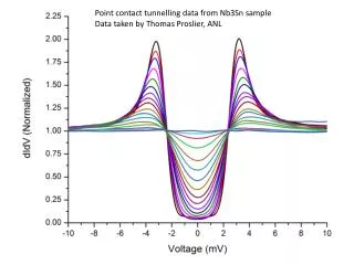
Δ Comparison SEM-EDX-PCT Γ/Δ
Comparison SEM-EDX Homogeneity composition in depth? 2.7 meV instead of 3 meV for Nb3Sn Nb rich surface---just oxide effect?
Attempt to do depth profiling Ag Nb3Sn Nb 7 kV electron beam -> Probing size ~ 300-330 nm (= step size for line scan) NOT CONCLUSIVE -> TEM NEXT
Transport Tc is taken at half the jump height Sheet Resistance (= ρ/thick) = 0.341 x Resistance

