AoE Project
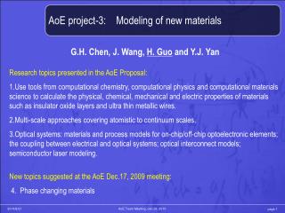
AoE Project. Nano -Process Modeling: Lithography modeling and device fabrication. Philip Chan, Mansun Chan Department of ECE, HKUST. Edmund Lam Department of EEE, HKU. Processing. The role of Processing Modeling. Lithography. Lateral Dimension (and variation). Post-Lithography

AoE Project
E N D
Presentation Transcript
AoE Project Nano-Process Modeling: Lithography modeling and device fabrication Philip Chan, Mansun Chan Department of ECE, HKUST Edmund Lam Department of EEE, HKU
Processing The role of Processing Modeling Lithography Lateral Dimension (and variation) Post-Lithography Processing Lateral/vertical Dimensions, dopant/substrate interaction Device Structure Structural parameters Device Characteristics Current-voltage, charge, transport, quantum characteristics Circuit Simulation Inter-connected devices characteristics
Lithography Layout and Lithography Layout 2D SEM 3D image Lithography is the driving force for scaling Lithography also becomes the major source of uncertainties *Mark E. Mason, DFM EDA Technology: A Lithographic Perspective, 2007 Symposium on VLSI Technology
Lithography Impact on Device Characteristics Gate length and parasitics variation Leakage, noise margin and power consumption variation currently modeled as many transistors in parallel in 22nm technology, need to account for atomic level variations Lithography models needed for Design for Manufacturing (DFM)
Lithography Potential Lithography Solutions *Source: ITRS Lithography 2008
Lithography Optical Projection Lithography *Source: A. Wong, Resolution Enhancement Techniques in Optical Lithography. SPIE Press, 2001. p. 24
Lithography Mask Design Forward problem: from mask design to circuit output Inverse problem: from circuit output to mask design
Lithography Mask Design Pre-distort the mask! needs optical system modeling • Optical proximity correction (OPC) • Rule-based and model-based mask circuit Source adjustment • Off-axis illumination (OAI) • Source-mask optimization (SMO)
Lithography Design for Manufacturing (I) Process variations e.g. focus, dose • Impact circuit behavior • Require “robust” design “original” “robust” mask infocus defocus
Lithography Design for Manufacturing (II) Mask manufacturability (cost) need “regularization” • Few segments • Rectilinear shapes • No close shapes (hotspots) unregularized regularized
post-Lithography Beyond Lithography Controlling vertical dimensions Further lateral dimension reduction The most common method to fabricate nanowire MOSFETs: stress limited oxidation Y. Tian, 2007 IEDM HKUST, EDL May 2009 CEA/LETI, IEDM 2008
post-Lithography Sidewall Etching Profile ♦Existing Model ♦Cannot explain the semicircular shape in single sidewall * R. Zhou, et. al., “Simulation of the Bosch process with a string-cell hybrid method”, J. of Micromechanics and Microengineering, v. 14 (2004), 851-858
post-Lithography The Etch-Deposition Model ♦Etching with deposition C4F8 – passivation agent SF6 – etching agent ♦deposited polymer only removed by the anisotropic component of the SF6 etchant ♦ final shape depends on the ratio of the etch rate versus deposition rate
post-Lithography Oxidation modeling ♦Can stress really limit the oxidation? ♦Experimental results show no limit at high temperature ♦No model can clearly capture these effects
post-Lithography Existing Model (Deal-Grove)
post-Lithography Crystal Orientation ♦Crystal orientation dependent oxidation has not been accounted for ♦Oxidation model has to be improved for non-planar devices due to multiple surfaces used
Devices Task DFM Objectives Lithography model Post-lithography processing model • Final geometry parameters • Effects of irregular cross-sectional geometry on device characteristics • Non-uniform quantum effects with non-circular/non-planar devices Model dependent intermediate device parameters Characteristic Variations
Tasks Lithography Modeling ♦Develop lithographic model, incorporating particularly parameters for the light source, and 3D mask effects ♦ Develop mask synthesis algorithms that are robustness against mask variations ♦ Incorporate regularization methods in solving inverse problems in imaging to tackle mask complexity ♦ Investigate the resulting parameter variations for input to the post-lithography processes
Tasks Etching/Oxidation Model ♦Develop post-lithography atomic etching model base on etching with co-deposition ♦ Experimentally verify the effect of stress on nano-scale oxidation ♦ Develop crystal orientation dependent oxidation model ♦ Incorporate the new models into a process simulator to predict the final shape of the device
Tasks Process-Aware Device Modeling ♦Study the impact of geometrical variation (e.g. non-uniform lateral dimension, non-ideal cross-section, atomic level dopant fluctuation) on the I-V characteristics including quantum effects ♦Develop model based with an orthogonal set of parameters that correlate the geometry data to electrical characteristics ♦Device fabrication and model verification
Tasks Second Phase of The Project ♦To Integrate the process models and device models to take in lithography process parameters and produce the corresponding device characteristics ♦ From the variations of process to predict the variation of device characteristics ♦ Develop inverse process algorithm to produce lithography patterns and process parameters to minimize the variation of device characteristics

