Download
1 / 29
290 likes | 496 Vues
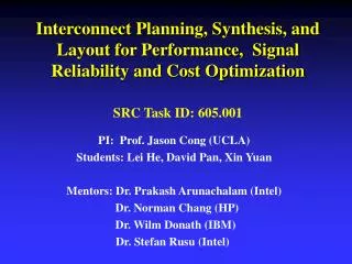
Interconnect Planning, Synthesis, and Layout for Performance, Signal Reliability and Cost Optimization SRC Task ID: 605.001. PI: Prof. Jason Cong (UCLA) Students: Lei He, David Pan, Xin Yuan Mentors: Dr. Prakash Arunachalam (Intel) Dr. Norman Chang (HP) Dr. Wilm Donath (IBM)

E N D
Interconnect Planning, Synthesis, and Layout for Performance, Signal Reliability and Cost OptimizationSRC Task ID: 605.001 PI: Prof. Jason Cong (UCLA) Students: Lei He, David Pan, Xin Yuan Mentors: Dr. Prakash Arunachalam (Intel) Dr. Norman Chang (HP) Dr. Wilm Donath (IBM) Dr. Stefan Rusu (Intel)
Objective: investigate an interconnect-centric design flow and methodology, consisting of: Interconnect Planning Interconnect Synthesis Interconnect Layout Project Overview
Three levels of planning: Interconnect architecture planning (pre-design) Interconnect planning with RTL-floorplan Interconnect planning with physical-level floorplan Enabling tools: interconnect estimation models for interconnect synthesis/layout Key Issues in Interconnect Planning
Efficient (constant time) and accurate (90%) interconnect delay estimation models for 2-pin nets under different interconnect optimization algorithms [Cong-Pan, IWLS’98, SRC/TECHCON’98, ASPDAC’99] Optimal wire sizing (OWS) Simultaneous driver and wire sizing (SDWS) Simultaneous buffer insertion/sizing and wire sizing (BISWS) Interconnect architecture planning [Cong-Pan,DAC’99] Propose a unified wire-width planning framework Obtain a surprising result that our pre-determined two-width can achieve close to optimal solution for a large wire length range ! Can handle different objective functions Review: Accomplishments in Year 1
Efficient and accurate interconnect estimation models for multiple-pin nets [Cong-Pan, TAU’99] Buffer block planning for interconnect-driven floorplanning [Cong-Kong-Pan, ICCAD’99] Further study on interconnect architecture planning Accomplishments in Year 2
Objective: estimate delay/area under different interconnect optimizations (e.g, OWS, BISWS) quickly (100K - 1M nets per second) Different targets: 1. Minimize the delay to a single critical sink (SCS) 2. Minimize the maximum delay (defined as the tree delay) for multiple critical sinks (MCS) Cs3 Cs1 G S1 S3 Sn G0 Csn S2 Input Cs2 Interconnect Estimation for Multiple-Pin Nets
Estimation for Multiple-Pin Nets • Very difficult: • No closed-form wire shaping or buffer insertion • All available optimization algorithms are iterative based • Multiple critical sinks may exist at the same time ! • Our approach • Reduce the multiple-pin net estimation problem into one or several 2-pin net estimation problems, then use our previous (Year 1) results
G0 G0 Input Input G Sk C1 Csk C2 Reduction for OWS of SCS Cs1 S1 G S3 Sk Csk S2 Cs2 Single-Line-Multiple-Load (SLML)
Transform SLML to SLSL (i.e., 2-pin net) OWS for SCS lk l2 l1 R d Sk W C1 C2 Ck Ck-1
C1 C2 Ck-1 OWS for SCS • Transform SLML to SLSL (i.e., 2-pin net) lk l2 l1 R d Sk W CL C0
Closed-form area estimation for the critical path Delay/Area Estimation for OWS/SCS • Closed-form delay estimation for the critical sink where , W(x) is Lambert’s W function defined as
Summary for Interconnect Estimation • Develop delay and area estimation models for multiple-pin nets with consideration of various interconnect optimizations • Consider different optimization objectives • Single critical sink (SCS) • Multiple critical sinks (MCS) • Apply various optimization alternatives: • Optimal wire sizing (OWS) • Buffer insertion/sizing and wire sizing (BISWS)
Delay/Area Comparison with TRIO • Rd = 180ohm, C1 = 100 fF, C2 = 10 fF • One internal load, l1 = 0.1 to 0.9 x l (l = 5, 10 or 20 mm) • Max. allowable wire width is 20x min. width; wire is segmented in every 10um.
Efficient and accurate interconnect estimation models for multiple-pin nets (Cong-Pan, TAU’99) Buffer block planning for interconnect-driven floorplanning (Cong-Kong-Pan, ICCAD’99) Further study on interconnect architecture planning Accomplishments in Year 2
For high-performance DSM designs, many buffers may be inserted to optimize/meet interconnect delay (e.g., up to 800,000 for 50nm tech., [Cong’97, SRC Work Paper]) The introduction of so many buffers will significantly change a floorplan; thus shall be planned to ensure timing/design convergence. Need proper buffer block planning (BBP) to address buffer location constraints (e.g., hard IP blocks) “dead area” utilization regularity for ease of layout and power/ground network sharing Motivation for BBP
Given: initial floorplan, buffer capacity for each soft block, and performance constraint for each net; Output: “optimal” location/dimension of buffer blocks such that the overall chip area and the number of buffer blocks are minimized. Buffer Block Planning Problem buffer blocks white space grey (soft) block (limited buffers) black (hard) block (no buffer allowed)
Feasible region is the maximal region that a buffer can be placed to meet given delay constraint. Feasible Regions for BI 1 buffer driver CL k buffers driver CL
We obtain the closed-form formula for FR’s Important observation: even under tight delay constraint, FR for BI can still be pretty large! => FR provides a lot flexibility to plan buffer location • FR distance under different delay budgets • Delay budget is (1+delta) Topt (the best delay by optimal buffer insertion) Feasible Regions for BI
FR extended to 2-dimension with obstacles 2-D FR Restricted (RES) line (delay minimal BI positions) Feasible Regions for BI sink source
1. Build polar graphs for given floorplan; 2. Build tile data structure; 3. For each tile, compute its area slacks; 4. Compute FR(s) for each net; 4. While (there exists some buffer to be inserted) { Pick_A_Tile that can insert most buffers w/o area penalty; if no such tile exists, pick the one with most BI demand ; Insert_Buffers into : insert all those buffers whose FR’s intersect with to create BB w/o area penalty; or insert one buffer into to expand its channel; Update chip dimension, FR, and area slacks, etc. } Overview of BBP Algorithm
Two Scenarios (for buffer insertion flexibility): RES: restricted buffer insertion position(s) as to minimize delay FR: feasible buffer region as to meet delay constraint Two Algorithms (for buffer clustering): RDM: a buffer is randomly assigned to any feasible location BBP: buffers are assigned with appropriate clustering 6 MCNC + 5 randomly generated circuits (0.18um tech) Experimental Setting
#nets that meet delay constraints FR provides a lot more flexibility than RES (e.g., to avoid obstacles) during BI, thus can better meet delay constraints
Area Increase (%) due to BI BBP/FR can effectively cluster individual buffers together with marginal area increase (less than 2% in all above test cases), by high utilization of “dead areas”.
Comparison of #BB BBP reduces #BB from RDM by a factor of up to 3x; BBP/FR further reduces #BB from BBP/RES by up to 34%
Efficient and accurate interconnect estimation models for multiple-pin nets (Cong-Pan, TAU’99) Buffer block planning for interconnect-driven floorplanning (Cong-Kong-Pan, ICCAD’99) Further study on interconnect architecture planning Our two width-planning is still valid for certain range (2x) of driver size variation Currently investigating wider range of variations Accomplishments in Year 2
Development of efficient and accurate interconnect performance estimation models for interconnect-driven synthesis and planning(Completed - 30-Jun-1999) Development of interconnect architecture planning framework (Completed - 30-Jun-1999) Development of efficient algorithms for integrated interconnect planning & floorplanning capabilities at the physical level (Completed- 30-Sep-1999) Development & validation of accurate noise models to guide the interconnect synthesis algorithm for signal reliability (Planned -31-Dec-1999) Development of optimal or near-optimal interconnect synthesis algorithm for multiple spatially or temporally related signal nets forperformance & signal reliability optimization (Planned - 31-Dec-1999) Development of efficient algorithms for integrated interconnect planning & floorplanning capabilities at the RTL-level; Software(Planned - 31-Dec-2000) Deliverables
TRIO (TRIO-Repeater-Interconnect-Optimization) package Integrated into Intel design technology Available on the web: http://cadlab.cs.ucla.edu/~trio IDEM (Interconnect Delay Estimation Model) package Prototype provided to Intel Package will be available this week to all SRC member companies: http://cadlab.cs.ucla.edu/~trio BBP (Buffer Block Planning) for physical level floorplanning Interest from Intel and HP Technology Transfer
Efficient and accurate interconnect estimation models Interconnect architecture planning Buffer Block Planning Future Work: Noise estimation and planning RTL interconnect planning Summary and Future Work
Development of a computational model for interconnect architecture planning based on a given design characterization (specified interms of target clock rate, interconnect distribution, depths of logic,network, etc.) (31-Dec-1998) Development of estimation models for interconnect layout optimizations suitable for pre-layout synthesis and planning(31-Dec-1998) Development of efficient algorithms for integrated interconnect planning and floorplanning capabilities at the RTL-level(31-Dec-1999) Completion of the ongoing effort on the development on a multi-layer general-area gridless routing system (31-Dec-1999) Development of optimal or near-optimal interconnect synthesis algorithm for multiple spatially or temporally related signal nets forperformance and signal reliability optimization (31-Dec-1999) Development and validation of very efficient but accurate noise models to relate the noise with the physical parameters to guide theinterconnect synthesis algorithm for signal reliability optimization (31-Dec-1999) Development of efficient algorithms for integrated interconnect planning and floorplanning capabilities at the physical level(31-Dec-1999) Development of efficient algorithms for integrated interconnect planning and floorplanning capabilities at the RT-level(31-Dec-2000) Milestones