On-Chip Scaled Power Combiner for Efficient CMOS Power Amplifiers
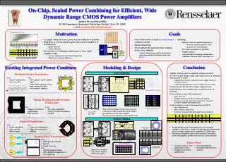
This work aims to analyze scaled, dynamic combiner systems for efficient and wide dynamic range CMOS power amplifiers. By reconstructing the signal envelope in the voltage domain, output voltages from each stage are scaled in a binary fashion. The goal is to quantify the effects of combiner parameters, determine optimal component values, and analyze non-idealities. The general model is technology-independent, suitable for on-chip or in-package integration. The study explores distributed active transformer series combining and parallel combining techniques, evaluating their pros and cons. Various transformer models and configurations, such as quarter-wave transformers and Figure-8 transformers, are discussed for optimizing efficiency and performance. Future work involves testing different combiner systems and investigating digital control interfaces for enhanced power control.

On-Chip Scaled Power Combiner for Efficient CMOS Power Amplifiers
E N D
Presentation Transcript
Goals • Goal of this work is to analyze scaled, dynamic combiner systems • Integrated solution • To reconstruct the signal envelope, scaling is in the voltage domain • Output voltages generated by each stage is scaled in an arbitrary fashion (in this case, binary) • Modeling • Quantify effects of combiner parameters • Determine optimal component values • Analyze effects of non-idealities • Investigate quasi-physical quantities • Simplify analysis • General model is technology independent (combiner can be on-chip, in-package, etc) On-Chip, Scaled Power Combining for Efficient, Wide Dynamic Range CMOS Power Amplifiers Andrew Pye and Mona Hella ECSE Department, Rensselaer Polytechnic Institute, Troy, NY 12180 e-mail: pyea@rpi.edu, hellam@rpi.edu Motivation * ITRS Roadmap 2006 – 2008 • As supply voltage decreases, power becomes difficult to maintain • High peak-to-average signals require linear power amplifiers to be backed off • Higher linearity • Lower efficiency • Discrete Power Combining combines power from scaled amplifier stages • Greater output power than from single stage • Maintains backed-off efficiency Decreasing breakdown voltage Existing Integrated Power Combiner Modeling & Design Conclusion Distributed Active Transformer Series Combining • Amplifier elements must be amplitude and phase matched • To achieve output voltage scaling, either input sources or combining elements must be scaled • Scaling sources requires scaling device sizes, supply voltages or matching networks • Scaling combining elements requires scaling reactance of lines • Scaling precision directly affects output voltage linearity • Input impedance varies significantly over different states of operation • Series combiner system (with transformer) • Easier to lay out • Winding inductance scaled by scaling factor squared • Performance depends upon finite quality factor of primary, secondary windings and coupling factor • Parallel combiner system (with lumped-element QWL) • More difficult layout • QWL scaled by scaling factor • Performance depends upon finite quality factor of inductor • Pros • Simple configuration • Low series loss • Cons • Only supports equal amplifier inputs • Large shunt capacitance from large transmission lines • Low magnetic coupling Transformer “T” Model Contour plot of system efficiency versus winding quality factors with series capacitor at output. kc = 0.7, N = 4 I. Aoki, S. Kee, D. Rutledge and Ali Hajimiri, “Distributed Active Transformer – A New Power-Combining and Impedance-Transformation Technique,” IEEE Transaction on Microwave Theory and Techniques, vol. 50, no. 1, pp. 316-331, Jan. 2002. Voltage-Boosting Parallel-Primary Transformer • Pros • Compact transformer configuration • High coupling • Cons • Not easily expandable • Large series loss in secondary winding • 130mm CMOS technology with three thick top metals • 3-stage binary weighted transformer-based combiner • Quasi-differential switch-mode amplifiers • Transmission gate shorts primary when amplifier is off System efficiency as a function of non-optimum secondary winding reactance. kc = 0.7, QP = 18, QS = 14 • VDD = 1.5V • RL = 50W K.H. Anj, Y. Kim, O. Lee, et al, “A Monolithic Voltage-Boosting Parallel-Primary Transformer Structures for Fully Integrated CMOS Power Amplifier Design,” IEEE Radio Frequency Integrated Circuits Symposium, 2007. Parallel Combining Figure-8 Transformer Differential QWL Model • Pros • Easily expandable • Low series loss • High coupling • Cons • Large area requirement • Large loss in secondary winding • The distribution of the total output power over multiple amplifiers, rather than a single stage will relax the requirements on the maximum output power capability of CMOS stages. • Switching off amplifier stages at lower power levels reduces power consumption, and therefore increase system efficiency 3-Turn OctagonalInductor P. Haldi, G. Liu, A. Niknejad, “CMOS Compatible Transformer Power Combiner,” IEE Electronics Letters, vol. 42, no. 19, pp. 1091-1092, Sept. 2006. Quarter-Wave Transformers • Pros • QWL provides isolation • Low loss • Simple structure GaAs die photo of PA with QWL parallel combiner Test Board for GaAs Amplifier Future Work • Construct and test series and parallel systems • Compare measured to modeled data • Investigate filtering • Investigate digital control interface 2-Turn Octagonal Coupled Inductor • Cons • Off-chip implementation • QWL difficult to implement at low frequencies • 250mm GaAs technology • 3-stage binary weighted QWL-based combiner * Simulation data Shirvani, et al, “A CMOS RF Power Amplifier with Parallel Amplification for Efficient Power Control,” IEEE J. Solid-State Circuits, vol. 37, no. 6, pp. 684—693, Jun. 2002