Understanding Output Voltage Clipping and Slew Rate in Non-Inverting Op-Amps
This guide explores the concepts of output voltage clipping and slew rate limitations in non-inverting operational amplifiers (op-amps). Using a practical example, we demonstrate how the maximum output voltage correlates with the input voltage and the impact of a slew rate of 0.5 V/µs on the output waveform. Additionally, we address factors influencing full-power bandwidth and DC imperfections such as input bias current and offset current, emphasizing the importance of these parameters for effective op-amp design and application.

Understanding Output Voltage Clipping and Slew Rate in Non-Inverting Op-Amps
E N D
Presentation Transcript
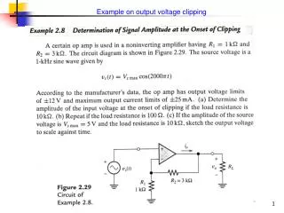
Closed loop gain of noninverting op amp (a) (b) Solving, we have V0, max = 2.44 V
(c) Clipping occurs at output voltage of 12 V or input voltage of 3 V
Slew-Rate Limitation As an example, assume we have a waveform, and we have to determine the output of the op-amp having a slew rate of 0.5 V/s
Full-Power Bandwidth The o/p voltage is: Taking derivative, we have: The maximum rate of the o/p voltage change is then equal to the slew rate: Thus the full-power bandwidth is: Thus, and undistorted full-amplitude sinusoidal voltage is possible only for frequencies less than fFP
DC Imperfections: Input bias current: Input offset current:
Model of op-amp with imperfections Unequal current flowing in the terminals and unequal voltages applied , as seen by an external source applied. Ideal op Amp