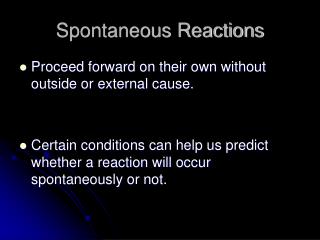
Spontaneous hydrophilic Si bonding
Latest Result Multiple Wafer Bonding Process Lixia Zhou, Matt Last Joseph M. Kahn Kristofer S. J. Pister October 16, 2002. Spontaneous hydrophilic Si bonding. Infrared picture of spontaneous wafer bonding. a) Start of bonding by applying a slight pressure, b) Extension after 2 sec,

Spontaneous hydrophilic Si bonding
E N D
Presentation Transcript
Latest ResultMultiple Wafer Bonding ProcessLixia Zhou, Matt LastJoseph M. KahnKristofer S. J. PisterOctober 16, 2002
Spontaneous hydrophilic Si bonding • Infrared picture of spontaneous wafer bonding. • a) Start of bonding by applying a slight pressure, • b) Extension after 2 sec, • c) Complete bonding after about 5 sec. • Maximum bonding wave velocity observed: 2 cm/s.
Why bonding? Scanning Mirror Veljko Milanovic, Matt Last, Kris Pister
Patterned SOI alignment bonding to realize multi-layer devices
PR SCS Wet Oxide Process flow I:
PR SCS Wet Oxide Process flow II:
PR SCS Wet Oxide Process flow III:
Problems coming across bonding • Ksaligner Si/Si bonding alignment accuracy is within +/- 30um. Design rule has to take care of this. • Bow/warpage of SOI wafer is preventing a secure bonding. Retaining an oxide layer on the back of handle wafer helps to reduce the bow. • Thermal stress from oxide membrane causes cracks and even breaks off part of the membrane during and after STS handle wafer etch. Having a thinner oxide membrane helps to reduce the stress.
* Comb drive pull_in * Compared with Veljko and Matt’s timed etch mirror: 20 degrees at 90V or 6 degrees at 56V. 1D scanning mirror: DC actuation
Testing structures pressure sensor pillar and roof bond strength measurement
Process works great! • High yield. • Need a more powerful simulation tool. • Problems associated with comb drive pull_in and 2D scanning mirror coupling can be solved with better design. • New design ideas are welcome. Microrobots? And what’s more?