Download

1 / 24
250 likes | 446 Vues
An Introduction to Carbon Nanotubes. Outline . History Geometry Rollup Vector Metallicity Electronic Properties Field Effect Transistors Quantum Wires Physical Properties Ropes Separation. CNFETs. Molecular. RTD. CNT arrays. Self assembled CNT using DNA. SETs. Quantum Dots.

E N D
Outline • History • Geometry • Rollup Vector • Metallicity • Electronic Properties • Field Effect Transistors • Quantum Wires • Physical Properties • Ropes • Separation
CNFETs Molecular RTD CNT arrays Self assembled CNT using DNA SETs Quantum Dots DNA strands as Bits Molecules in Solution DNA self assembly Molecular orientations as Bits What is Nanotechnology? • Switching devices of nanometer (below 100nm, typically 10nm) dimensions define nanotechnology. Emerging Nanotechnology Solutions Emerging Nanotechnology Drivers Logic (Our Focus) Nano CMOS Memory Fabrication
Computing Devices Solid State Devices Molecular Devices CMOS Devices Quantum Devices Nano CMOS Quantum Dot RTD CNFET SET Electro- mechanical Electro- chemical Quantum Photoactive
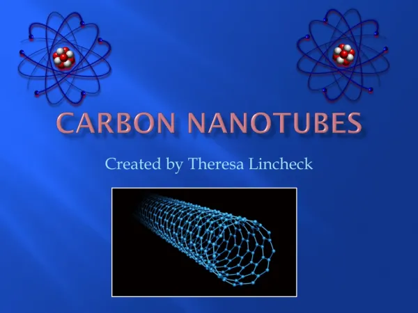
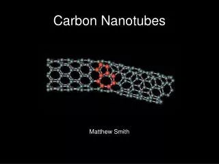
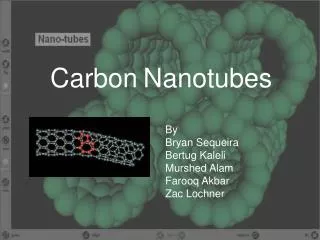
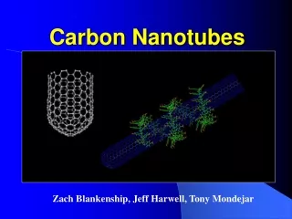
Introduction • High Aspect Ratio Carbon nanomaterial • Family inclues Bucky Balls and Graphene • Single Wall Carbon Nanotubes (SWCNT) • Multiwall Carbon Nanotubes (MWCNT)
History • 1952 L. V. Radushkevich and V. M. Lukyanovich • 50 nm MWCNT Published in Soviet Journal of Physical Chemistry • Cold War hurt impact of discovery • Some work done before 1991 but not a “hot” topic • 1991-1992 The Watershed • Iijima discovers MWCNT in arc burned rods Mintmire, Dunlap, and White‘s predict amazing electronic and physical properties • 1993 Bethune and Iijima independently discover SWCNT • Add Transition metal to Arc Discharge method (same method as Bucky Balls)
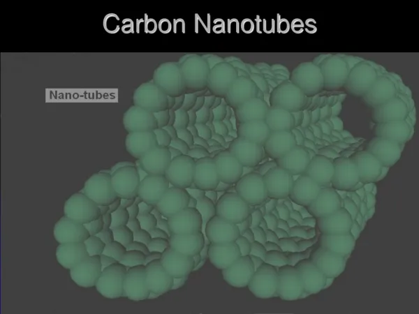
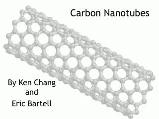
Carbon Nanotubes • Carbon nanotubes are long meshed wires of carbon • Longest tubes up to 1mm long and few nanometers thick made by IBM.
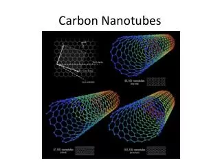
Geometry • Rollup Vector • (n,m) • n-m=3d • Chiral Angle • tan(θ) = √3m/(2√(n2+m2+nm)) • Arm Chair (n,n), θ=30 ○ • Zig-zag (n,0), θ=0 ○ • Chiral, 0○< θ<30 ○
Field Effect Transistors • FETs work because of applied voltage on gate changes the amount of majority carriers decreasing Source-Drain Current • SWCNT and MWCNT used • Differences will be discussed • Gold Electrodes • Holes main carriers • Positive applied voltage should reduce current
SWCNT Transport Properties • Current shape consistent with FET • Bias VSD = 10 mA • G(S) conductance varies by ~5 orders of magnitude • Mobility and Hole concentration determined to be large • Q=CVG,T (VG,T voltage to deplete CNT of holes) • C calculated from physical parameters of CNT • p=Q/eL
MWCNT Transport Properties • MWCNT performance is poor without defects • See arrow for twists in collapsed MWCNT • MWCNT has characteristic shape of FET • Hole density similar to SWCNT but Mobility determined to be higher • Determined same as above
FET Conclusions • Higher carrier density than graphite • Mobility similar to heavily p-doped silicon • Conductance can be modulated by ~5 orders of magnitude in SWCNT • MWCNT FET only possible after structural deformation
Quantum Wires • SWCNT Armchair tubes • SWCNT deposited over two electrodes • Electrode resistance determined with four point probe and found to be ~ 1 MΩ
Coulomb Charging • Contact Resistance Lower than Rquantum=h/e2~26 kΩ • C very low s.t. EC=e2/2C very large • If EC <<kT, Current only flows when Vbias>EC • Various gate V taken into account • Step-like conductance
Quantum Wire • Strongly Temperature dependent conduction curve • Occurs when a discrete electron level tunnels resonantly though Ef of electrode • If electron levels of SWCNT where continuous peak would be constant • E levels separated by ΔE • The resonant tunneling implies that the electrons are being transported phase coherently in a single molecular orbital for at least the distance of the electrodes (140 nm)
Physical Properties of Ropes • SWCNT rope laid on ultra-filtration membrane • AFM tip applies force to measure Shear Modulus G and Reduced Elastic Modulus Er • Er = Elastic Modulus when Searing is negligible • Displacement of tube/Force was measured and Er and G where calculated
Summary of Results • Typical Values • Gdia ~ 478 GPa • Ggla ~ 26.2 GPa • Er-dia ~ 1220 GPa • Er-gla ~ 65-90 GPa
Conclusion On Physical Properties • Shear properties of SWCNT lacking (Even compared to MWCNT ropes) • Elastic properties very promising
Synthesis and Seperation • One major reason CNT devices have been so hard to scale up to industry uses is due to the inability to efficiently separate different species of CNT • Different types are produced randomly with 1/3 conducting 2/3 semiconducting • It has now been reported that with the use of structure-discriminating surfactants one can isolate a batch of CNT such that >97% CNT within 0.02 nm diameter
Overview of Technique • Surfactants change buoyancy properties of CNT • Ultra-centrifugation techniques (which are scale-able) are used to separate different CNT • Effective separation is seen • Separation according to metallicity • Separation according to diameter
Conclusion • CNT devices show promise in molecular electronics both as wires and FET • Physical properties are very promising being both strong and light • Separation techniques continue to be developed to allow companies to make CNT devices
CNT-based nanomotor CNT-based bio-probe Nanotube oscillator IC integrated CNT CNT Devices
Molecular Electronics Nanotube Nanowire Arrays (Lieber et al., Harvard) TubeFET (McEuen et al., Berkeley) Nanotube Logic (Avouris et al., IBM Research)
1 mm Length Scale Wl: boundary scattering W lF: quantized effects Ll: ballistic transport - W + - L Size of a Microprocessor MEMS Devices 1 mm Thin Film Thickness in ICs 100 nm l (Mean free path at RT) 10 nm Nanotube/ Nanowire Diameter 1 nm lF(Fermi wavelength) Atom 1 Å