Investigating Phonon-Induced Changes in Electrical Resistance of Conducting Oxides
This research explores how phonons—vibrations of the crystal lattice—scatter electrons in nano-scale electronic devices, impacting the electrical resistance of conducting oxides. We focus on the interaction between SrTiO3 and LaSrMnO3. Our findings reveal that phonons from SrTiO3 can propagate across atomically-thin interfaces and significantly affect electron scattering in LaSrMnO3, revealing a sharp increase in resistance. This discovery provides crucial insights into the atomic-scale properties of conducting oxides and their potential applications in advanced electronic devices.

Investigating Phonon-Induced Changes in Electrical Resistance of Conducting Oxides
E N D
Presentation Transcript
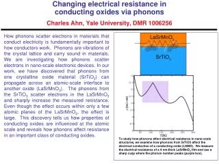
Changing electrical resistance in conducting oxides via phononsCharles Ahn, Yale University, DMR 1006256 How phonons scatter electrons in materials that conduct electricity is fundamentally important to how conductors work. Phonons are vibrations of the crystal lattice and carry sound in materials. We are investigating how phonons scatter electrons in nano-scale electronic devices. In our work, we have discovered that phonons from one crystalline oxide material (SrTiO3) can propagate across an atomic-scale interface to another oxide (LaSrMnO3). The phonons from the SrTiO3 scatter electrons in the LaSrMnO3 and sharply increase the measured resistance. Even though the effect occurs within only a few atomic planes of the LaSrMnO3, the effect is large. This discovery tells us how properties of conducting oxides are influenced at the atomic scale and reveals how phonons affect resistance in an important class of conducting oxides. O To study how phonons affect electrical resistance in nano-scale structures, we examine how phonons from SrTiO3 affect the electrical conduction of a conducting oxide (LSMO). We measure the electrical resistance of a 4 nm-thick LaSrMnO3 film and see a sharp cusp where the phonon number peaks (purple box).
Imaging a ferroelectric-silicon transistor using transmission electron microscopyCharles Ahn, Yale University, DMR 1006256 Ferroelectric transistors are complex devices that require state-of-the art synthesis, device fabrication, and characterization techniques. Development of these devices provides several opportunities for undergraduate student participation. Successful function of the devices requires smooth interfaces, which can be imaged in cross section using transmission electron microscopy (TEM). Rohan Harrison, an undergraduate from Southern Connecticut State University, prepared cross section samples of films grown at Yale and found smooth and sharp interfaces between the individual components of the transistor. Glue Gold PZT STO 200 nm Si Undergraduate Rohan Harrison (SCSU) carries out TEM evaluation of the single crystal ferroelectric oxide (PZT) grown on top of silicon (Si) using advanced physical vapor deposition techniques. A thin SrTiO3 buffer layer is used to match the PZT to Si.