Variation
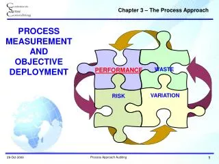
Variation. Sources of Variation. Process (manufacturing) (physical) variations: Uncertainty in the parameters of fabricated devices and interconnects From die to die Within a particular die Environmental (operating context) (temporal) (dynamic) variations:

Variation
E N D
Presentation Transcript
Sources of Variation • Process (manufacturing) (physical) variations: • Uncertainty in the parameters of fabricated devices and interconnects • From die to die • Within a particular die • Environmental (operating context) (temporal) (dynamic) variations: • Uncertainty in the operating environment of a particular device during its lifetime • Temperature • Supply voltage • Lifetime wear-out
Temperature Variation Within die temperature variation • Temperature Variation: • Both the device and interconnect performance have temperature dependence, • Higher temperature performance degradation.
Process Variation • Process variation: Sample space: • Set of manufactured dies • Results in yield loss • Y = # working die / # manuf. Die • A small portion of sample space is allowed to fail timing constraints • CPU/GPU design: Speed/core binning: for different applications • Lessens the requirement that all or very high percentage of die meets the fastest timing constraint
Process Variation [Cadence]
Environmental Variation • Environmental Variation: Sample space: • Operational life of a chip • A pessimistic analysis is required • Should ensure correct operation throughout lifetime • Design that operates faster than necessary for much of its operational life • loss in efficiency • One approach: • Runtime adaptivity of the design • Environmental Variation: Treated by worst case analysis • Process variation: Treated statistically
Process Variation: Sources • PV Sources: • Var. in physical parameters (due to imperfect manufacturing): • Gate length or critical dimension (CD) • Gate oxide thickness • Channel doping concentration • Interconnect thickness • Interconnect width • … • Dominant factors: CD and channel doping • Var. in electrical parameters of components • Vth • Drive strength of transistors • Resistance of wires • Capacitance of wires • …. • Var. in circuit characteristics: • Delay • Power • Noise
x 10-7 2.3 2.2 2.1 2.0 1.9 1.8 60 100 40 50 20 Wafer X Wafer Y 0 Process Variation Sources [IBM, Intel and TSMC]
Process Variation • A physical parameter variation may affect more than one electrical parameter: • Wire width • Wire capacitance • Wire resistance • Coupling noise • Gate oxide thickness • Drive current • Vth • Cg
Correlation Must consider correlation between electrical parameters • If ignore correlation (Cw, Rw), • In theory, both may be at worst–case values • Impossible in practice • Correlation among physical parameters themselves • An equipment variation (e.g. lens deviation) may impact multiple physical parameter values (all metal layers and poly) • Hard to model due to large number of equipment-related parameters • Most algorithms take physical parameters to be basic random variables
Classification • Types of physical-parameter variations: • Systematic (deterministic): • Show predictable variational trends across a chip • Caused by known physical phenomena during manufacturing • Can be predicted upfront by analyzing the designed layout • Can be avoided in final stages • E.g. Metal fill, optical proximity effects • But at early stages, common to be treated statistically - E.g.,regions with uniform metal densities have more uniform ILD thicknesses - Most of the time, not available to designers/CAD developers
Classification • Types of physical-parameter variations: • Non-systematic (random): • Truly uncertain component of physical-parameter variations • Resulted from processes that are statistically independent of the design implementation • Only the statistical characteristics are known at design time, • Must be modeled using RVs • Common practice: • In earlier stages, both systematic and nonsystematic variations are modeled statistically • As we move through the design process and more detailed information is obtained, the systematic components can be modeled deterministically (if sufficient analysis capabilities are available)
Scaling Effect • A 4nm MOSFET predicted in mass production in 2020, • < 10 Si atoms are expected along the channel (IBM roadmap) • MOS transistors are rapidly becoming truly atomistic devices • Random variations are becoming dominant. • A 22nm MOSFET expected in mass production • 50 Si atoms along the channel • Large parameter fluctuations
Classification • Classification of variation: • Die-to-die (inter-die) (global): • Affects all devices on the same die in the same way • Within-die: WID (intra-die) (local) (on-chip: OCV): • Affects each device on the same die differently • E.g. some devices have larger/smaller CDs than nominal
D2D Variation [Menezes07]
Classification • Types of within-die variation: • Spatially-correlated: • Many of the underlying processes that give rise to within-die variation change graduallyfrom one location to the next. • Affect closely spaced devices in a similar manner • Make them more likely to have similar characteristics than those placed far apart • Independent: • Statistically independent from all other devices • Scaling Contribution of independent within-die variation is increasing • With SC: • Leff, • Temperature • Supply voltage • No SC: • tox, • Dopant concentration
Inter-die vs. Intra-die Variations Inter-die global Correlation Leff Intra-die spatial Correlation • Figures are courtesy of IBM, Intel and TSMC
References • [Blaauw08] Blaauw, Chopra, Srivastava, Scheffer, “Statistical Timing Analysis: From Basic Principles to State of the Art,” IEEE Transactions on CAD, Vol. 27, No. 4, April 2008. • [Forzan09] Forzan, Pandini, “Statistical static timing analysis: A survey,” Integration, The VLSI Journal, 42, 2009. • [Menezes07] Menezes, “The Good, the Bad, and the Statistical,” Invited talk, ISPD 2007.


