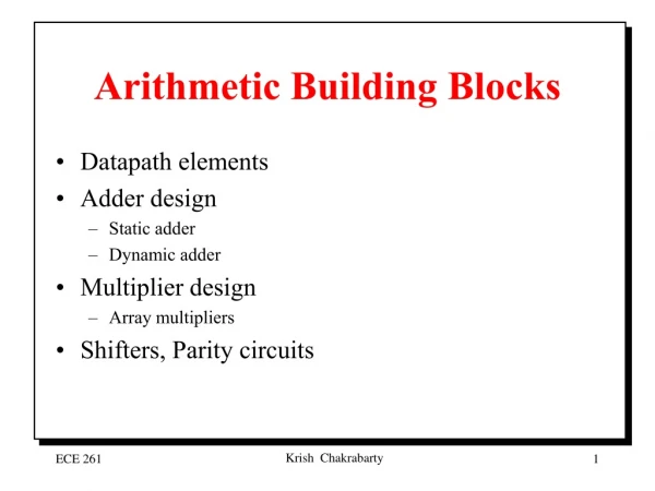
Arithmetic Building Blocks
Arithmetic Building Blocks. A Generic Digital Processor. Building Blocks for Digital Architectures. Arithmetic unit. Bit-sliced datapath. adder. -. (. , multiplier,. shifter, comparator, etc.). Memory. - RAM, ROM, Buffers, Shift registers. Control.

Arithmetic Building Blocks
E N D
Presentation Transcript
Building Blocks for Digital Architectures Arithmetic unit Bit-sliced datapath adder - ( , multiplier, shifter, comparator, etc.) Memory - RAM, ROM, Buffers, Shift registers Control - Finite state machine (PLA, random logic.) - Counters Interconnect - Switches - Arbiters - Bus
The Mirror Adder • The NMOS and PMOS chains are completely symmetrical. This guarantees identical rising and falling transitions if the NMOS and PMOS devices are properly sized. A maximum of two series transistors can be observed in the carry-generation circuitry. • When laying out the cell, the most critical issue is the minimization of the capacitance at node Co. The reduction of the diffusion capacitances is particularly important. • The capacitance at node Co is composed of four diffusion capacitances, two internal gate capacitances, and six gate capacitances in the connecting adder cell . • The transistors connected to Ci are placed closest to the output. • Only the transistors in the carry stage have to be optimized for optimal speed. All transistors in the sum stage can be minimal size.
Single-Bit Addition Half Adder Full Adder For the Sum Sk If Ak=Bk then Sk=Ck-1 else Sk=Ck-1 For the carry If Ak=Bk then Ck=Ak=Bk else Ck=Ck-1
Implementing ALU Function with an Adder Sk=HkCk-1 + HkCk-1 Ck=AkBk+HkCk-1 Hk=AkBk +AkBk
Carry Select Adder For a n-bit ripple carry adder, Completion time T=k1n, where k1 is delay through one adder cell. For Carry select adder the completion time T=Pk1 + (M-1)k2, Where the n-bit adder is divided in M blocks and each block contain P adder cell and k2 is the delay through the multiplexer. Mopt=(nk1/k2)
Carry Skip Adder Worst case carry propagation for carry skip addeer The total (worst case) propagation delay time T is given by T=2Pk1 + (M-2)k2 Mopt=(2nk1/k2)
The Array Multiplier X0 X1 X2 X3 Y0 X2 X3 X1 X0
The MxN Array Multiplier— Critical Path Critical Path 1 & 2