JOHN G. EKERDT
80 likes | 105 Vues
This research focuses on studying the growth and properties of ultrathin metal, dielectric, and ferroelectric films for optical and electronic applications. The research also examines the catalytic conversion of lignin to chemicals. Topics of investigation include nucleation and growth of films and nanostructures, structure-property relationships, and site-specific reactions.

JOHN G. EKERDT
E N D
Presentation Transcript
JOHN G. EKERDT RESEARCH FOCUS We study surface and materials chemistry as it relates to the growth and properties of ultrathin metal, dielectric and ferroelectric films for optical and electronic applications, and we study the catalytic conversion of lignin to chemicals. We seek to understand and describe nucleation and growth of films and nanostructures, structure-property relationships, and site-specific reactions.
Current Group/Collaborators Funding: AEC, Intel Corp., NSF, ONR, Welch
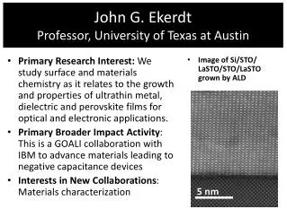
ALD growth of high-k dielectric and expitaxial oxides Primary Goal:Stabilize the amorphous phase of HfO2; Grow expitaxial oxides on epi-surfaces prepared by MBE Photocatalyst TiO2 on SrTiO3-buffered Si Atomic Layer Deposition (ALD) of amorphous high-k dielectric Molecular Beam Epitaxy (MBE) system • Amorphizing elements (La, Al, Ta, etc.) can be incorporated into HfO2 to increase the film crystallization temperature • The distribution of the amorphizer also affects film crystallization temperature Anatase TiO2 ALD XPS/UPS SrTiO3 [4Hf+1La]×32 STM Cross-sectional TEM of TiO2 on SrTiO3 LaCoO3 on SrTiO3-buffered Si grown using MBE with atomic oxygen Strain from SrTiO3 induces a ferromagnetic state in LaCoO3 that can possibly be exploited for novel devices ALD system (to be connected with the MBE) Large changes in bond lengths and angles due to strain Customized ALD chamber, ensuring in situ sample transfer and high efficiency deposition
Validate the predictions for Ru and Co films using P and B grown from the hydrides PH3 and B2H6, and determine how properties scale with thickness Nucleation Promotion: Control of the nucleation behavior of Pt on HOPG is achieved through the use of Boron implantation to create defect sites, altering the number of nuclei formed and the final structure of the material. Poor nucleation: Good nucleation: Ultrathin Continuous Metal Films Primary Goal: Examine the nucleation, deposition, and material properties of thin metal films, with a focus on the control of composition and nucleation. Annealed 6L HOPG <0360> Amorphous Ru(P) Model Increased B2D6 exposure leads to trap sites that increases the number of particles forming on HOPG
Nanoparticle nucleation on oxides Primary Goal: Determine the chemical nature of native and synthesized defects on oxides and use this knowledge to control particle nucleation on these materials. Stable cluster at defect site Defect Site Left: Plot of areal density versus Si dose showing influence of etching on density. Below: SEM images of Ge particles on SiO2 exposed to no (b) and 1.0 ML (f) Si etching. Schematic of nucleation processes on surfaces with defect sites that are capable of trapping adatoms. Smaller clusters are stable at trap sites, increasing the total nuclei density. Stable Cluster Defect chemistry and structure: Fluorescent molecules with specific functional groups (vectors) bind to defect sites on these materials. Photoluminescence (PL) spectra can then provide direct information about the types and density of defects. Defect mediated nucleation: Particle density can be controlled by creating surface defects that can act as traps for adatoms. Defect concentration is controlled on SiO2 by etching with Si. Ge particle density can be enhanced by an order of magnitude with this method. PL spectra from compounds deposited on silica after heating to ~525 K for the perylene dosed sample and ~ 750 K for the 3-vinyl perylene dosed sample.
Biomass Processing in Ionic Liquids Primary Goal: Develop methods for separation, depolymerization, and hydro-deoxygenation of lignin for use as a fuel or aromatic feedstock in ionic liquids Ionic liquids Biomass Fuel, Chemicals • Can dissolve biomass • Tuneable properties • No vapor pressure • Can act as solvent/catalysts Lignin Cellulose/ hemicellulose Acid catalyzed depolymerization Hydrodeoxygenation Phenylalkanes Lignin fragments ■ Conversion □Yield Remove heteroatomes while maintaining aromatic character Testing various catalysts and conditions is the next step in the project • Up to 82.5% yield • Anion influences reaction mechanism • Acidity of ionic liquids measured
iCVD Deposition of Conformal Polymer Primary Goal: Utilize iCVD deposition techniques to create a nanoscale, conformal polymer coating as a responsive surface layer in a small RFID sensor Interdigitated Circuit (from collaborator: Neikirk, UT) Ge Nanowire Paper (from collaborator: Korgel, UT) Initiated Vapor Phase Polymerization + + Monomer (Vinyl Pyridine) Ferrite “core” Crosslinker (Divinylbenzene) Initiator (di-tert-butyl peroxide) Interdigitated pattern allows very high capacitance sensors Nanowire mats have very high surface area to volume ratios, ideal for a sensor substrate iCVD deposition allows conformal coating even in deep wells and sub-micron gaps The iCVD Reactor The coating type will determine sensitivity of the sensor: Aromatic: polystyrene Straight-chain oil: polyethylene Salinity: polyacrylate pH: polymethacrylic acid Complete Sensor (coated nanowires atop circuit)