Download
1 / 49
490 likes | 506 Vues
This project aims to develop large-area detectors with space and time resolution for various applications. The collaboration includes national labs, divisions, and electronics expertise from universities and small companies. The goal is to create commercializable modules within a 3-year R&D period.

E N D
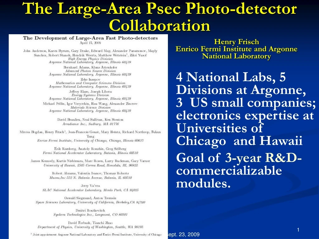
The Large-Area Psec Photo-detector Collaboration Henry Frisch Enrico Fermi Institute and Argonne National Laboratory 4 National Labs, 5 Divisions at Argonne, 3 US small companies; electronics expertise at Universities of Chicago and Hawaii Goal of 3-year R&D- commercializable modules. DOE Site Visit Sept. 23, 2009
The Development of Large-area Detectors With Space and Time Resolution OUTLINE • Application Space: Four frontiers- time resolution, area, QE, and cost (different applications sit at different points in this 4D space, but not separated by large amounts of development effort- all 4 are fertile.) • The LAPPD Collaboration: present status, and introduction to the posters and breakout session • Challenges and Surprises (e.g., funding has been available at ANL for only 1 month- not yet available at SSL, Hawaii, UC, Arradiance, Minotech, Muons,Inc, Synkera,…) DOE Site Visit Sept. 23, 2009
Motivationand Requirements DOE Site Visit Sept. 23, 2009
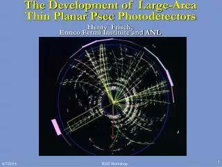
At colliders we measure the 3-momenta of hadrons, but can’t follow the flavor-flow of quarks,the primaryobjects that are colliding. 2-orders-of-magnitude in time resolution would all us to measure ALL the information=>greatly enhanced discovery potential. Application 1-Energy Frontier Specs: Signal: 50-10,000 photons Space resolution: 1 mm Time resolution 1 psec Cost: <100K$/m2: t-tbar -> W+bW-bbar
Application 2- Lepton Flavor Physics • Example- DUSEL detector with 100% coverage and 3D photon vertex reconstruction. • Need >10,000 square meters (!) (100 ps resolution) • Spec: signal single photon, 100 ps time, 1 cm space, low cost/m2 (5-10K$/m2)* (Howard Nicholson) * Hermetic DUSEL specs TBD DOE Site Visit Sept. 23, 2009
Application 3- Medical Imaging (PET) Reminder- mention new iniative in France for PET and Hadron Therapy using these ideas- US should not have to follow….. Depth of interaction measurement; 375 ps resolution (H. Kim, UC). (note distinguished ANL/UC history in medical imaging, esp. PET) Spec: signal 10,000 photons,30 ps time, 1 mm space, 30K$/m2, MD-proof DOE Site Visit Sept. 23, 2009
Application 4- Nuclear Non-proliferation • MCP’s loaded with Boron or Gadolinium are used as neutron detectors with good gamma separation (Nova Scientific). • Large-area means could scan trucks, containers • Time resolution corresponds to space resolution out of the detector plane IF one has a t_0– i.e can do 3D tomography of objects Specs: Unknown An area for possible applications- need a counterpart to form an application group. DOE Site Visit Sept. 23, 2009
SUMMARYCharacteristics in common we need • Small feature size << 300 microns • Homogeneity – the ability to make uniform large-areas (think solar-panels, floor tiles, 50”-HDTV sets) • Intrinsic low cost: although application specific, all need low-cost materials and robust batch fabrication. Need to be simple. DOE Site Visit Sept. 23, 2009
PET (UC/BSD, UCB, Lyon) Collider (UC, ANL,SLAC,.. DUSEL (Matt, Mayly, Bob, John, ..) K->pnn (UC(?)) Security (TBD) Parallel Efforts on Specific Applications Explicit strategy for staying on task . LAPD Detector Development ANL,Arradiance,Chicago,Fermilab, Hawaii,Muons,Inc,SLAC,SSL/UCB, Synkera, U. Wash. Drawing Not To Scale (!)
Using New Technologies to Exploit Fundamentally Simple Ideas DOE Site Visit Sept. 23, 2009
Detector Development- 3 Prongs MCP development- use modern fab processes to control emissivities, resistivities, out-gassing Use Atomic Layer Deposition for emissive material (amplification) on cheap inert substrates (glass capillary arrays, AAO). Scalable to large sizes; economical; pure – i.e. chemically robust and stable. Readout: Use transmission lines and modern chip technologies for high speed cheap low-power high-density readout. Anode is a 50-ohm stripline. Scalable up to many feet in length ; readout 2 ends; CMOS sampling onto capacitors- fast, cheap, low-power. Use computational advances -simulation as basis for design Modern computing tools allow simulation at level of basic processes- validate with data.
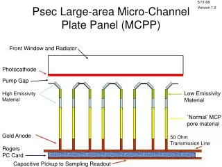
Micro-channel Plates PMTs Satisfies small feature size and homogeneity Photon and electron paths are short- few mm to microns=>fast, uniform Planar geometry=>scalable to large areas DOE Site Visit Sept. 23, 2009
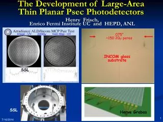
Simplifying MCP Construction Conventional Pb-glass MCP OLD Incom Glass Substrate NEW Chemically produced and treated Pb-glass does 3-functions: • Provide pores • Resistive layer supplies electric field in the pore • Pb-oxide layer provides secondary electron emission Separate the three functions: • Hard glass substrate provides pores; • Tuned Resistive Layer (ALD) provides current for electric field (possible NTC?); • Specific Emitting layer provides SEE DOE Site Visit Sept. 23, 2009
Glass Substrate Status ANL, Chicago, Incom, Minotech, SSL • Have received multiple samples of 10-micron, 20-micron, 40-micron glass substrates from Incom in 3/4”-sq and 33 mm round formats (latter the SSL/ANL development format) • Incom has ordered 8”x8” shell- they are sharing development cost (largely paying for it, in fact) • Incom is refining 8”x8” process- changes to draw, grinding, polishing. Very responsive to our needs, very flexible. DOE Site Visit Sept. 23, 2009
Self-Assembled Passive Substrates AAO Group: Hau Wang (ANL), Dmitry Routkevitch (Synkera)+postdoc, Synkera • Alternative to glass capillary substrate- parallel path. • Some advantages: batch production (could be very cheap), inherent purity, low radioactivity • May naturally allow funnel geometry with reflection photocathode (could be very very fast and cheap) • Longer development path, at present glass is priority DOE Site Visit Sept. 23, 2009
Functionalization- ALD ALD Group: Jeff Elam, Anil Mane, Qing Peng, Thomas Proslier (ANL:ESD/HEP), Neal Sullivan (Arradiance), Anton Tremsin (Arradiance, SSL) Jeff Elam, Thomas Proslier DOE Site Visit Sept. 23, 2009
Functionalizing Incom samples ALD Group: Jeff Elam, Anil Mane, Qing Peng, Thomas Proslier (ANL:ESD/HEP), Neal Sullivan (Arradiance), Anton Tremsin (Arradiance, SSL) Jeff Elam, Thomas Proslier (ESD) ALD film Cross-sectional EDAZ of JE1401a ALD ZnO and AL203 extend into pores Sputtered Au only on edge of pores SEM from Middle of JE1401a 100 nm ALD film visible in middle of MCP DOE Site Visit Sept. 23, 2009
ALD-Functionalized substrates Picture is seam between blocks Jeff Elam, Thomas Prolier (ESD) DOE Site Visit Sept. 23, 2009
MCP and Photocathode Testing First measurements of gain in an ALD SEE layer at the APS laser test setup (Bernhard Adams, Matthieu Cholet, and Matt Wetstein) Testing Group: Bernhard Adams, Matthieu Cholet, and Matt Wetstein at the APS, Ossy Siegmund’s group at SSL N. B.! LAPPD Preliminary (very)
Characterization of Secondary Emission, Photo-Emission of Materials Characterization Group: Igor Veryovkin, Thomas Proslier, Alexander Zinovev (MSD), postdoc (meets biweekly, joint with photocathode group- perhaps ALD gp too in the future.) • Constructing dedicated setup for low-energy SEE and PE measurements of ALD materials- parts on order. (will see on tour in Bld 200). Goal is systematic exploration of best SEE materials • Has parts-per-trillion capability for characterizing photocathodes after exposure to Argon, MCP’s before&after scrubbing, aging. Goal is to avoid having to scrub, aging- it is essential to measure and understand the surface chemistry. • Planning interfaces to SSL, APS vacuum systems, common sample database • Has close ties/overlap with ALD and testing groups
Photocathode Group Photocathode Group: Klaus Attenkofer(APS), Sharon Jelinsky(SSL), Jason McPhate(SSL), Mike Pellin (MSD), Ossy Siegmund (SSL), Thomas Proslier(MSD), Zikri Yusof(HEP), postdoc (meets biweekly, joint with characterization group) Work is going on on multiple fronts- the photo-cathode is probably the most complex area we are dealing with. Bialkali photocathodes are not hard to make, have good QE and a spectral response well matched to water cherenkov counters and most optical applications. We (will) have a strong effort on them at SSL, which has the experience and a long track record. This will ensure having a solution as good as typical commercial tubes. At the same time, there is a strong case to be made that there can be substantial improvements in QE (see Townsend’s paper), spectral matching, and possibly chemical robustness. In addition, MCP’s may allow reflection rather than transmission cathodes, with big gains in speed (sub-psec) and QE. There may be new ideas based on ALD, e.g., (see Mike Pellin’s, Greg Engel’s talks at Photocathode workshop) that are feasible and disruptive. We are reaching out to university groups to access high-end facilities and young talent- UIUC, UIC, and WashU. (Yes, risky, but high payoff- if not us, who? see Chu, Koonin) DOE Site Visit Sept. 23, 2009
SSL Photocathode Group Sharon Jelinsky(SSL), Jason McPhate(SSL), Ossy Siegmund (SSL), • Sealed tubes with up to 5” format havebeen processedwith multialkaliphotocathodes • MCPs and delayline readout From Ossy Siegmund’s talk at the First Photocathode Workshop, July 20-21, Univ. of Chicago/ANL DOE Site Visit Sept. 23, 2009
MCP Simulation- use to make informed decisions on materials, geometry, field,… Simulation Group: Zikri Yusov, Valentin Ivanov (Muons,Inc), Sergey Antipov (HEP), Zeke Insepov (MCSD) , Anton Tremsin (SSL/Arradiance ), Neal Sullivan (Arradiance)
MCP Simulation • Zeke Insepov (MCSD) and Valentin Ivanov (Muons,Inc) DOE Site Visit Sept. 23, 2009
MCP Simulation • Zeke Insepov (MCSD) and Valentin Ivanov (Muons,Inc) DOE Site Visit Sept. 23, 2009
MCP Simulation • Zeke Insepov (MCSD) and Valentin Ivanov (Muons,Inc) DOE Site Visit Sept. 23, 2009
Front-end Electronics/Readout Waveform sampling ASIC Electronics Group: Jean-Francois Genat, Gary Varner, Mircea Bogdan, Michael Baumer, Michael Cooney, Zhongtian Dai, Herve Grabas, Mary Heintz, James Kennedy,Sam Meehan, Kurtis Nishimura,Eric Oberla, Larry Ruckman, Fukun Tang (meets weekly) First have to understand signal and noise in the frequency domain DOE Site Visit Sept. 23, 2009
Front-end Electronics Resolution depends on 3 parameters: Number of PhotoElectrons, Analog Bandwidth, and Signal-to-Noise Wave-form sampling is best, and can be implemented in low-power widely available CMOS processes (e.g. IBM 8RF). Low cost per channel. See J-F Genat, G. Varner, F. Tang, and HF arXiv: 0810.5590v1 (Oct. 2008)- now published in Nucl. Instr. Meth. DOE Site Visit Sept. 23, 2009
Front-end Electronics/Readout Waveform sampling ASIC prototype • Varner, Ritt, DeLanges, and Breton have pioneered waveform–sampling onto an array of CMOS capacitors. DOE Site Visit Sept. 23, 2009
First 0.13micron ASIC due back Oct. 20 The chip submitted to MOSIS -- IBM 8RF (0.13 micron CMOS)- 4-channel prototype. Plan on 16 channels/chip- possibly 32 later (??). DOE Site Visit Sept. 23, 2009
Get position AND timeAnode Design and Simulation(Fukun Tang) • Transmission Line- readout both ends=> pos and time • Cover large areas with much reduced channel account. • US Patent DOE Site Visit Sept. 23, 2009
Photonis Planicon on Transmission Line Board Couple 1024 pads to strip-lines with silver-loaded epoxy (Greg Sellberg, Fermilab). DOE Site Visit Sept. 23, 2009
Comparison of measurements (Ed May and Jean-Francois Genat and simulation (Fukun Tang) • Transmission Line- simulation shows 3.5GHz bandwidth- 100 psec rise (well-matched to MCP) • Measurements in Bld362 laser teststand match velocity and time/space resolution very well
Scaling Performance to Large AreaAnode Simulation(Fukun Tang) • 48-inch Transmission Line- simulation shows 1.1 GHz bandwidth- still better than present electronics. KEY POINT- READOUT FOR A 4-FOOT-WIDE DETECTOR IS THE SAME AS FOR A LITTLE ONE- HAS POTENTIAL… DOE Site Visit Sept. 23, 2009
ANL Test-stand Measurements Jean-Francois Genat, Ed May, Eugene Yurtsev Sample both ends of transmission line with Photonis MCP (not optimum) 2picoseconds; 100 microns measured DOE Site Visit Sept. 23, 2009
Test Fixture for integration of ASIC and transmission-line anode being designed ``Both parts are completely routed and ready for submission after pinout check etc.” Illustration of how we operate- close Hawaii/UC collaboration on ASIC, system design. Larry Ruckman (Hawaii)- From our electronics blog (open to all- go to http://hep.uchicago.edu/psec) Test fixture for OptionE glass anode interface to first proto-type sampling ASIC – test bandwidth, reflections, cross-talk.
Mechanical Assembly Mechanical Group: Dean Walters (NE), Rich Northrop (UC), Henry Frisch (UC), Michael Minot (Minotech Eng.), Greg Sellberg (Fermilab) Ossy Siegmund (SSL), Anton Tremsin (SSL/Arradiance), R. Wagner (HEP)+0.5postdoc, Sam Asare (UC), Rahul Barwhani (UCB) Group meets weekly Ongoing work on: • Sealing- tray options A,C,E; window seal • Anode fabrication, testing • Sealed-tube considerations- outgassing, getters, surface-physicsAssembly- • Vacuum assembly/Alternatives • Cost (a driver for everything) DOE Site Visit Sept. 23, 2009
Cartoon of the `Frugal’ MCP • Put all ingredients together- flat glass case (think TV’s), capillary/ALD amplification, transmission line anodes, waveform sampling DOE Site Visit Sept. 23, 2009
In principle, can dial size for occupancy, resolution- e.g. neutrinos 4’by 2’ This is not what we will do first…. DOE Site Visit Sept. 23, 2009
Mechanical Assembly 8” proto-type stack Design sketch 8” proto-type mock-up DOE Site Visit Sept. 23, 2009
Mechanical Assembly 8” proto-type- stresses Luckily we have access to the world’s most sophisticated test facilities at Argonne and UC Lead bricks DOE Site Visit Sept. 23, 2009
Moreover, we have Ossy and his group • This talk has focused on Argonne- however we are lucky to have Ossy Siegmund’s group at SSL working in parallel (on a subcontract- still trying to get him the funds!!) on using his proven technologies to make bialkali photocathodes and ceramic-body MCP’s. • Ossy has a wealth of knowledge and experience, and brings a healthy skepticism to our trying to be faster, better and cheaper (`pick any 3’ is the old engineering adage, pace Dan Goldberg). • In parallel we are trying to develop what Paul Horn (IBM) calls a `disruptive technology’-higher risk, but high payoff. Cheap glass envelope/anode , possibly pure gas assembly, mass production with no burn-in. DOE Site Visit Sept. 23, 2009
Administration Transparency/Dissemination Administration Group: Karen Byrum (co-PI), Henry Frisch (co-PI), Bob Wagner (Project Physicist), Dean Walters (Project Engineer) • Weekly all-subgroup meeting (Tues at 10 am) • Web site has Blogs used for weekly meeting- open to the world. Has played a significant role in interfacing to small technical companies (both reassuring and also interesting them). See http://hep.uchicago.edu/psec/ • Web site has Library of our talks, papers, internal notes, documents, backup materials,etc,- again, goal is to be transparent and accountable. • We have been running >= 2 workshops/year, 1 in Chicago, 1 in France. Very influential on a wide community-we benefit from contacts DOE Site Visit Sept. 23, 2009
Internal Review Panels (open to additional suggestions). • Introduced on CDF- worked very very well. DOE Site Visit Sept. 23, 2009
First Collaboration Meeting DOE Site Visit Sept. 23, 2009
First Year Milestones DOE Site Visit Sept. 23, 2009
Challenges and Surprises(Places we need help)(note: this is personal list from HJF with UC/EFI hat on- not a criticism of ANL-on the contrary, I’m blown away by the breadth, depth, and quality at ANL) SSL, Hawaii, UC, Arradiance, Minotech, Muons,Inc, Synkera have not gotten a single dime yet. Folks are working, but not getting paid- purchase orders are waiting. (systemic problem- not a complaint about personnel or any office). We had not counted on it’s being Oct. or later to start. Ossy’s operation on photocathodes and ceramic-based anodes is the biggest schedule risk. We had thought we would have access to a fully functioning glass shop at ANL. Being worked on by management, but delay and risk in schedule. Alternatives in local industries being developed, but in-house is much more flexible and effective for R&D. Subcontracts cost a 15% overhead bite right off the top. Ossy’s budget in particular got hit by an 84K$ cut. Perhaps in later years one could go directly to SSL? (can this be made up in some way?)
The End- DOE Site Visit Sept. 23, 2009
BACKUP DOE Site Visit Sept. 23, 2009