TD5102 Embedded System in Silicon
TD5102 Embedded System in Silicon. FPGA Architecture and EDA Dr. Ha Yajun ( E1-08-17, e lehy@nus.edu.sg ) http://courses.nus.edu.sg/course/elehy/TD5102/. Embedded Systems.

TD5102 Embedded System in Silicon
E N D
Presentation Transcript
TD5102 Embedded System in Silicon FPGA Architecture and EDA Dr. Ha Yajun (E1-08-17,elehy@nus.edu.sg) http://courses.nus.edu.sg/course/elehy/TD5102/
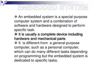
Embedded Systems • An embedded system is nearly any computing system (other than a general-purpose computer) with the following characteristics • Single-functioned • Typically, is designed to perform predefined function • Tightly constrained • Tuned for low cost • Single-to-fewer components based • Performs functions fast enough • Consumes minimum power • Reactive and real-time • Must continually monitor the desired environment and react to changes • Hardware and software co-existence Yajun Ha / ECE, NUS
Embedded Systems • Examples: • Communication devices • Wired and wireless routers and switches • Automotive applications • Braking systems, traction control, airbag release systems, and cruise-control applications • Aerospace applications • Flight-control systems, engine controllers, auto-pilots and passenger in-flight entertainment systems • Defense systems • Radar systems, fighter aircraft flight-control systems, radio systems, and missile guidance systems Yajun Ha / ECE, NUS
Problem Partitioning Algorithm Functional Modeling Software Func. Model Hardware Func. Model Architectural synthesis Application Source Code Structural RTL HDL Simplified and General Embedded System Design Methodology SW/HW Interface Algorithms Software Development Application Specific Hardware(ASIC/FPGA) Processors Platforms SW/HW Interface Yajun Ha / ECE, NUS
+ > + > * - - * Configuration Sw + > * - Three Kinds of Embedded SystemImplementation Platform Choices Processor Reconfigurable FPGA Hardwired ASIC D$ Rf +|-|*|>| ID I$ Sw Configurable Parallel wired algorithm “Program” flow (occasionally) Distributed data Programmable Sequential Instruction flow (cycle) Transfer bottleneck No wiring No configuration Overhead Power: 100 10 1 Yajun Ha / ECE, NUS
Why Use Reconfigurable Hardware? Processor- Processor- Processor ASIC FPGA Performance Low High Medium Flexibility High Low High Power High Low Medium Why FPGAs ? • Combine flexibility with performance. • Shorter time-to-market and longer time-in-market. • #FPGA gates/USD: 2004 1 M/10$. • FPGA capacity: now 2004 50Mgates => FPGAs get used as functional part of a design (<-> prototyping) Yajun Ha / ECE, NUS
Embedded Software Tools CPU Logic + Memory + IP +Processors + RocketIO (Virtex-II Pro) CPU Embedded Software Tools Embedded Software Tools FPGA + Memory + IP + High Speed IO (4K & Virtex) Logic Design Tools FPGA Programmable Systems usher in a new era of system design integration possibilities I/O Logic Design Tools Memory Logic Design Tools Integration in System Design Integration of Functions Time Yajun Ha / ECE, NUS
FPGA Based Reconfigurable Platform • Reconfigurable Platforms Architectures • EDA for Reconfigurable Architectures • Applications of Reconfigurable Platforms • Lab Sessions on FPGA Board Yajun Ha / ECE, NUS
Simplified FPGA Architecture Functional Block All the three components can be re-programmed with configurations to implement application-specific digital circuits. For example, each functional block can be programmed to implement a small amount of digital logic of a design; the routing network can be programmed to implement the design specific interconnection pattern; I/O blocks can be programmed to implement the input and output ports according to design requirements. Routing Network I/O Block Yajun Ha / ECE, NUS
FPGA Reconfiguration • All the programming information for the three programmable RA components is stored in a configuration file. The configuration file for a RA is often called a bitstream compared to a binary executable for a processor. Once a bitstream for a digital logic design is downloaded to a RA, the RA is programmed to implement the design. By providing different bitstreams, a single RA can be re-programmed to implement different designs at different times. Bitstream File 1 Time 1 Time 2 Bitstream File 2 Yajun Ha / ECE, NUS
Local Inter- connect LE Functional Block Inputs Functional Block Outputs LE ….. LE Functional Block Internals FPGA Functional Block Our target RAs use the Look-Up Table (LUT) type of functional block. Such a functional block is normally made of one or several logic elements (LE). They differentiate from each other mainly in terms of the input size of a LE and the number of LEs in a functional block. State-of-the-art RAs normally use 4-input LEs. Yajun Ha / ECE, NUS
FPGA Logic Element LE Internals The LE consists of a 16 SRAM cell Look-Up Table (LUT), and a flip flop (FF). The 16 SRAM cells LUT stores the truth table of any 4-input logic function, thus it can implement any 4-input logic function. The FF implements the storage element in a sequential circuit. Yajun Ha / ECE, NUS
LUT Content ABCD F F = A*B+C*D The 16 SRAM cell LUT stores the output column of the truth table of the F function. The 4 inputs A, B, C and D will determine which bit the F value is for the current values of A, B, C and D. Yajun Ha / ECE, NUS
Additional Computational Resources • Besides the LEs present in previous slide, some functional blocks in different target RAs have architecture specific features to improve the performance when implementing arithmetic functions. • These architecture specific features include carry logic, embedded memory blocks, multiplier and other hard cores. • Hard cores generally implement functions efficiently compared to FPGA functional blocks. Memory blocks Microprocessor blocks Yajun Ha / ECE, NUS
FPGA Routing Architecture A logic block input or output pin can connect to some or all of the wiring segments in the channel adjacent to it via a connection block of programmable switches. At every intersection of a horizontal channel and a vertical channel, there is a switch block. It is a set of programmable switches that allow some of the wire segments incident to the switch block to be connected to others. By turning on the appropriate switches, short wire segments can be connected together to form longer connections. Yajun Ha / ECE, NUS
FPGA Routing Wires • Some target RAs contain routing architectures that include different lengths of wires. • The length of a wire is the number of functional blocks it spans. • Left figures show wires of length 1, 2 and 4. Yajun Ha / ECE, NUS
XC4000 Routing Architecture Example Yajun Ha / ECE, NUS
Commercial FPGA Architecture Comparison Yajun Ha / ECE, NUS
IBM CoreConnect™ on-chip bus standard PLB, OPB, and DCR RocketIO Dedicated Hard IP DSOCM BRAM ISOCM BRAM Flexible Soft IP PowerPC 405 Core DCR Bus Instruction Data PLB OPB Bus Bridge Arbiter Arbiter Processor Local Bus On-Chip Peripheral Bus e.g. Memory Controller Hi-Speed Peripheral GB E-Net On-Chip Peripheral UART GPIO Off-Chip Memory ZBT SRAM DDR SDRAM SDRAM PowerPC-based Embedded Design Full system customization to meet performance, functionality, and cost goals Yajun Ha / ECE, NUS
MicroBlaze 32-Bit RISC Core Possible in Virtex-II Pro LocalLink™ FIFO Channels OPB On-Chip Peripheral Bus Arbiter 0,1…….32 Custom Functions Custom Functions On-Chip Peripheral 10/100 E-Net UART MicroBlaze-based Embedded Design I-Cache BRAM Local Memory Bus Flexible Soft IP BRAM Configurable Sizes D-Cache BRAM Off-Chip Memory FLASH/SRAM Yajun Ha / ECE, NUS
FPGA Based Reconfigurable Platform • Reconfigurable Platforms Architectures • EDA for Reconfigurable Architectures • Applications of Reconfigurable Platforms • Lab Sessions on FPGA Board Yajun Ha / ECE, NUS
FPGA Design Flow Yajun Ha / ECE, NUS
Time Profile for Design Flow Steps Logic Optimization and routing steps normally consume the major part of the design flow time. Yajun Ha / ECE, NUS
FPGA Technology Mapping Technology step restructures the primitive logic gates, generated from the logic optimization step, into sets of 4-input functional blocks. Yajun Ha / ECE, NUS
FPGA Placement and Routing The placement step finds physical locations for functional blocks, while the routing step finds physical routes for logic connections. Yajun Ha / ECE, NUS
Embedded Design in an FPGA • Embedded design in an FPGA consists of the following: • FPGA hardware design • C drivers for hardware • Software design • RTOS versus Main + ISR Yajun Ha / ECE, NUS
Standard FPGA HW Development Flow VHDL/Verilog Synthesizer Simulator Place & Route ? Download to FPGA Embedded DevelopmentTool Flow Overview Standard Embedded SW Development Flow C Code Compiler/Linker (Simulator) Object Code ? CPU code in off-chip memory CPU code in on-chip memory Download to Board & FPGA Debugger Yajun Ha / ECE, NUS
Embedded Development Kit • The Embedded Development Kit (EDK) consists of the following: • Xilinx Platform Studio – XPS • Base System Builder – BSB • Create and Import Peripheral Wizard • Hardware generation tool – PlatGen • Library generation tool – LibGen • Simulation generation tool – SimGen • GNU software development tools • System verification tool – XMD • Virtual Platform generation tool - VPgen • Software Development Kit (Eclipse) • Processor IP • Drivers for IP • Documentation • Use the GUI or the shell command tool to run EDK Detailed data sheet of Xilinx FPGA devices and user manuals of ISE and EDK tools are available online at http://www.xilinx.com/support/library.htm Yajun Ha / ECE, NUS
FPGA Based Reconfigurable Platform • Reconfigurable Platforms Architectures • EDA for Reconfigurable Architectures • Applications of Reconfigurable Platforms • Lab Sessions on FPGA Board Yajun Ha / ECE, NUS
--- Quoted from Cindy’s Boy Friend!!! Why Networked Hardware? Cindy Crawford asked me to encrypt our mobile phone talk!!! It is not an easy job!!! So I resort to hardware. But one day Cindy cried and told me that our talk had been disclosed. I laughed and said “Baby, never mind, I will change the encryption instantly through the network!!!” Yajun Ha / ECE, NUS
Future Networked Applications Need Client Platforms with Flexible Hardware Acceleration • Future networked applications can require high computing power up to 1000 Giga Ops [Nakatsuka, ISSCC’99], thus hardware acceleration is generally needed, and networked applications will contain both software and hardware components. • Different networked applications may use different industry standards to support new services, and require the client platforms to be flexible. • Networked applications usually work with a server-client model, and require the client platforms to be connected to the network. Yajun Ha / ECE, NUS
ISP1 ISP2 ISPN Distr. memoryarch. Application Description Dowloading static interconnect network HW Part ASIC Reconfigurable Hardware SW Part • Both ISP and reconfigurable HW can be programmed to adapt changing standards. • Reconfigurable HW can provide a better than ISP energy efficiency of high processing power vs. power consumption. • Configurations for both ISP and reconfigurable HW can be network downloaded. flexible! High computing power! networked! Target Client Platform: Networked Reconfigurable Platform Yajun Ha / ECE, NUS
ISP1 ISP2 ISPN Distr. memoryarch. Application Description Up to 16 serial transceivers Dowloading static interconnect network HW Part ASIC Reconfigurable Hardware SW Part PowerPCs • Both ISP and reconfigurable HW can be programmed to adapt changing standards. • Reconfigurable HW can provide a better than ISP energy efficiency of high processing power vs. power consumption. • Configurations for both ISP and reconfigurable HW can be network downloaded. flexible! ReConfig. logic High computing power! Courtesy of Xilinx (Virtex II Pro) networked! Commercial FPGA Platform Yajun Ha / ECE, NUS
ISP1 ISP2 ISPN Distr. memoryarch. static interconnect network ASIC Re-configurable Hardware Networked SW/HW Reconfiguration of Networked Information Appliance User Selects App User Downloads App Advertise App on Web Page Web Page Description Dowloading HW File Java File Yajun Ha / ECE, NUS
Web MPEG Video Player Java MPEG Player + IDCT bitstream CPU + FPGA Client Web Page Client Side Server Side Yajun Ha / ECE, NUS
Networked Reconfiguration is Better Service Client Service Provider Service Request network Service II Data Streams Service I Reconfig Info Service II Reconfig Info Service I Data Streams …... Yajun Ha / ECE, NUS
FPGA Based Reconfigurable Platform • Reconfigurable Platforms Architectures • EDA for Reconfigurable Architectures • Applications of Reconfigurable Platforms • Lab Sessions on FPGA Board • Lab Session 1: Reconfigurable fabric based hardware design • Lab Session 2: Processor+Reconfig Fabric based system design Yajun Ha / ECE, NUS
MEMEC Virtex-4 LC FPGA Board Serial Port FPGA Push Buttons DIP Switches LEDs More FPGA board related documentations have been put online at http://courses.nus.edu.sg/course/elehy/EE4218/projects.htm Yajun Ha / ECE, NUS
FPGA Board Demo • When PUSH2 (SW5) is not held down, the 7-segment display (DD1) does a binary-to-hex conversion of the binary number represented by the 4-bit DIP switch (SW3). • When PUSH2 (SW5) is held down, the 7-segment display (DD1) counts from 0-9. • LED1, LED2, LED3, and LED4 count in binary from 0-9 (matching what is on DD1 when PUSH2 is pressed). • Pushing PUSH1 resets the counter. 7-segment Display SW5 PUSH2 Yajun Ha / ECE, NUS
FPGA Lab 1 & 2 • Please print relevant docs by yourself and bring to labs! • Watch the FPGA board demo closely • Lab 1: Try to re-implement the demo with Xilinx ISE on your FPGA board and do the assignment • Design files for the demo will be installed on your PC. • You need to use Xilinx ISE tool to generate and download the bitstream. • Get familiar with Xilinx ISE environment and link the various FPGA design flow steps to the tool. • Browse and understand the design files for the demo. • Lab 2: Follow the Xilinx EDK tutorial that can be found in the TD5102 course web site under project page. Lab session in Signal Processing and VLSI Lab (E4-08-34) 2:00-5:00pm on 13 & 14 Dec! Yajun Ha / ECE, NUS
Summary • FPGA architectures have been introduced. • EDA tools for FPGAs have been introduced. • Applications of FPGA for networked platforms have been introduced. • Lab introduction. Yajun Ha / ECE, NUS