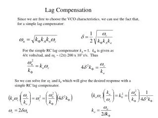
Lag Compensation
Lag Compensation. Since we are free to choose the VCO characteristics, we can use the fact that, for a simple lag compensator:. For the simple RC lag compensator k A = 1. k F is given as 4/ p volts/rad, and w n ~ (2 p ) 200 x 10 3 r/s. Thus.

Lag Compensation
E N D
Presentation Transcript
Lag Compensation Since we are free to choose the VCO characteristics, we can use the fact that, for a simple lag compensator: For the simple RC lag compensator kA = 1. kF is given as 4/p volts/rad, andwn~ (2p) 200 x 103 r/s. Thus So we can solve for wcand k0which will give the desired response with a simple RC lag compensator.
For the simple RC lag compensator, H(s) = wc/(s+wc). The closed loop transfer functions to the phase detector output (T1) and the VCO input (T2) are: To find the step responses, multiply the transfer functions by 1/s and take the inverse Laplace Transforms:
Lag Compensated Phase Detector Response Lag Compensated VCO Response
Lead-Lag Compensation Since we are free to choose the VCO characteristics we must choose VCO gain to satisfy For the simple RC lead-lag compensator kA = 1. kF is given as 4/p volts/rad, andwn~ (2p) 200 x 103 r/s. Thus Surprise! We can now step through the lead-lag compensator design per the method presented in class. It is interesting to note that if we set k0 = wn/2dkF, as we did with the simple lag compensator, the zero (w2) moves to infinity, and w1 = wcfrom the lag approach.
For the simple RC lead/lag compensator, H(s) = (w1/ w2)(s+w2)/(s+w1). The closed loop transfer functions to the phase detector output (T1) and the VCO input (T2) are: To find the step responses, multiply the transfer functions by 1/s and take the inverse Laplace Transforms. Note that the form of T1 and T2 is exactly the same as T1 for the simple lag network phase detector output with w1 or w2 substituted for wc .
Lead-Lag Compensated Phase Detector Response Lead-Lag Compensated VCO Response
Answers to In-class Exam • 1a Enough information exists in that bandwidth to make voice intelligible. • 1b 6.6 k-samples/sec • 1c Avoid aliasing • 1d 52,800 bits/sec • 1e Nonlinear gain characteristic where low levels are boosted before A/D conversion and restored after D/A conversion at the receiver. Improves S/N for low volume levels . • 2a 25 channels • 2b 100 channels • 2c Baud rate is symbol rate, symbols may contain multiple bits/symbol. • 2a-biphase: 1200Kbaud, 1200K bit/sec 2b-16 QAM: 1200Kbaud, 4800K bit/sec • 2d Takes a much larger noise phasor to cause an error in biphase than 16 QAM • 3 BW = 37.5 Khz for all. 2-phase: 75K bit/sec, 3-phase: 118.9 K bit/sec, 4-phase: 150K bit/sec • 4 FEC adds redundant information to a digital message so that transmission errors can be corrected at the receiver. The theory tells us we can construct FEC codes to correct an arbitrary number of errors, given enough redundancy, reducing the probability of error to near zero. • 5 -- 01 10 11 11 10 01 00 10 00 01 11 01 01 00 10 01 –- • 1 0 0 1 1 1 1 0 1 0 0 1 0 1 1 1 • 6a “COMM IS KOOL” • 6b Even Parity • 6c 4th bit in “K” . . Should be “C” • 6d 80.77%