ITO
Sodium β-alumina as a High-k Solution-processed Gate Layer for Transparent and Low Voltage Electronics Howard E. Katz, Johns Hopkins University, DMR 1005398 Studies of Na+ ion polarization, and 0905176, x-ray diffraction .

ITO
E N D
Presentation Transcript
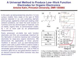
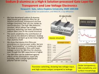
Sodium β-alumina as a High-k Solution-processed Gate Layer for Transparent and Low Voltage ElectronicsHoward E. Katz, Johns Hopkins University, DMR 1005398Studies of Na+ ion polarization, and 0905176, x-ray diffraction • We have developed sodium β-alumina (SBA)-based gate dielectric films for all solution-processed, transparent and low voltage transistors that use zinc oxides as semiconductors. The high SBA dielectric constant, which allows low voltage transistor switching, has been ascribed to sodium (Na+) ions in the crystal structure • This work establishes the contribution of Na+ ions to the dielectric behavior, leading to dielectric constant up to ten times higher than alumina itself. • We show that device thin films are amorphous on macroscopic scales, but are likely “precrystalline” on molecular scales. This leads to smoother films with lower leakage current for SBA than for alumina, even though the SBA capacitance is higher. • The SBA films can be stabilized against effects of the atmosphere, especially humidity, with a simple hydrophobic polymer barrier coating Al electrode ZTO Sodium beta alumina Device structure ITO Oxide transparency, SBA crystallinity, and surface morphology Transistor switching, showing low voltage input, and high current output compared to leakage
Broad Impacts-- Sodium β-alumina/ZnO Transistors Howard E. Katz, Johns Hopkins University, DMR 1005398 • All solution-processed, transparent and low voltage transistors are important for window-mounted displays and sensors using low power and covering large areas. • We have established a collaboration with Hanbat University in Daejeon, South Korea to print electronically active oxide inks based on our materials, and presented our results at an international symposium at that university (upper photo) • We have advanced the scientific careers of three minority undergraduate students from Howard University and Prince Georges Community College through their participation in this project (lower photo) • We have incorporated oxide device fabrication in an undergraduate classroom laboratory module now used yearly in a JHU electronic materials laboratory course and which has been disseminated to three other universities • A publication has appeared: Zhang, B.; Liu, Y.; Agarwal, S.; Yeh, M.; Katz, H.E. “Structure, Sodium Ion role, and Practical Issues for β-alumina as a High-k Solution-processed Gate Layer for Transparent and Low Voltage Electronics” ACS Appl. Mat. Int. 3, 4254-4261 (2011)