Download
1 / 29
290 likes | 371 Vues
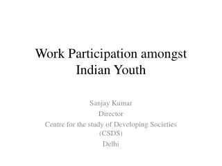
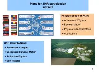
INDIAN PARTICIPATION @ FAIR Subhasis Chattopadhyay. The future Facility for Antiproton an Ion Research (FAIR). Primary beams: 10 12 /s 238 U 28+ 1-2 AGeV 4 · 10 13 /s Protons 90 GeV 10 10 /s U 35 AGeV (Ni 45 AGeV) Secondary beams: rare isotopes 1-2 AGeV antiprotons up to 30 GeV.

E N D
INDIAN PARTICIPATION @ FAIR Subhasis Chattopadhyay
The future Facility for Antiproton an Ion Research (FAIR) Primary beams: 1012 /s 238U28+ 1-2 AGeV 4·1013/s Protons 90 GeV 1010/s U 35 AGeV (Ni 45 AGeV) Secondary beams: rare isotopes 1-2 AGeV antiprotons up to 30 GeV SIS 100 Tm SIS 300 Tm cooled antiproton beam: Hadron Spectroscopy Ion and Laser Induced Plasmas: High Energy Density in Matter Structure of Nuclei far from Stability low-energy antiproton beam: antihydrogen Compressed Baryonic Matter
The Story: Brainstorming meeting on Nuclear Physics in next 20 years (DST-DAE meet @Mumbai (7-8 April 2006) Committee for FAIR: S. Chattopadhyay, VECC (Coordinator) S. Bhattacharya, SINP D. Biswas, BARC L.M. Pant, BARC S. Mandal, DU R. Palit, TIFR
Guidelines: • Contribution should make impact on overall physics • Contribution should be on specific hardware • HW should be built in the country • Early contact should be made to the main experiment • Collaboration is the key with large university participation • Should have significant spin-off • Detailed e-mail discussion • Meeting at BARC/VECC • Co-ordinators for respective experiments • Report send on October’end-2006
Official status • DST-DAE co-ordination committee meet (july 07) • V.S. Ramamurthy: Chairman, FAIR-India task force • DST meeting took place on Dec 30th 2007 • ( Finance Secy cleared the project) • VSR attended FAIR meet at GSI • DST-DAE co-ordination committee meet could not be taken • twice, next scheduled on 8th March’08
Building the SuperConducting Magnets for SUPER-FRS And Building of proton LINAC components (Major contributions, in-kind)
BC1 BC2 BEAM CATCHERS BC3 To stop primary beam & other fragments
Implementation Strategy of FAIR Project (Time ~ 4 yrs) • Design at VECC • Design verification at VECC and GSI • Prototype built by VECC in INDIA • Test run at GSI • Formulation of final beam dump design • Fabrication in INDIA • Installation in Super FRS Beam Line at GSI
4 dipole 4 quadrupoles 1 sextupole
Milestones: • Mid of 2007: Magnetic design of dipole magnet • Mid of 2008: Engineering design of dipole magnet • End of 2009: Fabrication of full size dipole magnet • Mid of 2011: Fabrication of additional 3 dipole magnets • End of 2007: Magnetic design of quadrupole magnet • End of 2008: Engineering design of quadrupole magnet • Mid of 2010: Fabrication of full size quadrupole magnet • End of 2011: Fabrication of additional 3 quadrupole magnets, one sextupole magnet
Other experiments: NUSTAR PANDA
Our Achievements So far (1988-2007)… • PMDs for WA93,WA98, STAR,ALICE, Muon chambers for ALICE • Development of advanced gaseous detector laboratory • * Gaseous detector laboratory exist at VECC-SINP and other collaborating institutes • (3) Development of advanced electronics laboratories • (MANAS development, a highlight) • (4) Development of large scale computing facilities (Grid computing) • (5) Successful International and National Collabotation • (VECC,SINP,PU,RU,JU,IOP,AMU,IIT-Bombay) • (6) More than 40 PhD students Future based on this strong base of experience and expertise
INDIA-CBM COLLABORATION Collaborators: VECC SINP IOP BARC Panjab U Rajasthan U AMU Calcutta Univ BHU Jammu Univ Guahati Univ Kashmir Univ IIT-KGP Bose-Inst, Kolkata … Simulate, design, build and operate a large part of CBM muon system • Three (Indian) collaboration meetings so far • Last on 30-31st July’07 at VECC • Discussed details of physics/HW/simulation • Simulation is running at VECC and at other • places • One GEM-based chamber built and tested • with source • One Engineer visited GSI for electronics work
Development of fast, highly granular muon detector for Compressed Baryonic Matter experiment @FAIR MuCh detector 2007 20 20 20 30 35 cm • Beam : 2015 • Distance – 2.6 m • Chambers: high • resolution gas detectors • (entire Indian effort) • Challenges: • High Rate • High density • Large background 260cm Fe Fe Fe Fe Fe 5 cm 0 cm 102.5 cm
Comparison of detectors.. Both GEM & MICROMEGAS are suitable for high rate applications
GEM (fast high resolution detector) stack under test GEM assembly housed in ~60 cm x ~30 cm box Gas Inlet Resistive chain biasing Gas: Ar/CO2-70/30 Source: Ru106(ß) mesh – a 5-10 micron thick nichrome wire source 6 mm holes in the plexiglass top cover for Source. Micron (30micron) level hole
Electronics • (Plan to participate in design and development of fast electronics) • One engineer visited GSI, • started working on a FPGA-based readout board • Discussion started on participation in design of n-XYTER chip • (32MHz, 128 channels) • Calcutta University wants to participate in a big way A. Roy and M. Dey will give details
Development of ASIC for CBM readout chip. • n-XYTER chip: • (mixed mode) • 128 channels • 32 MHz rate (analog) • Useful for all purpose applications • GSI has assigned part of the design job to us • Discussion started at CU and BARC design team
Thick GEM, (first attempt) 0.5mm thick double-sided copper clad FR4 material. hole size is 0.3mm and the pitch is 1.2mm. Made locally.
Near term PLAN : 0.5mm x 0.5 mm readout plane, to be readout by GASSIPLEX GASSIPLEX Board +DAQ ready Readout plane ready Next: with n-XYTER??
Next Steps.... • to do a gain estimation with the double GEM ....maybe implement a third GEM layer • Operate with a segmented readout – PCB ready • Do timing Study, and for that one may try to optimise or use the already optimized gas mixture for high rates • Use THGEM, as it more robust • Testing a MICROMEGAS foil. • Build facility at BHU
Simulation • Codes installed (Partha’s talk tomorrow) • Immediate plan: • Muon trigger study • Magnetised Iron as absorber • Optimisation of detector/absorber combination • Radiation study with FLUKA
Plan (as put in DST-DAE proposal): Detector development and control: VECC, SINP, BHU, PU, JU Electronics: VECC, CU, BARC Simulation: VECC, GU, JU, BHU, PU, AMU Silicon layer : BARC