Materials for Interconnects and Contacts in Microelectronics
Learn about metallization materials for high-performance microelectronics, including aluminum, copper, gold, polysilicon, refractory metals, and silicides. Explore techniques for forming ohmic contacts and addressing challenges like the Kirkendall effect.

Materials for Interconnects and Contacts in Microelectronics
E N D
Presentation Transcript
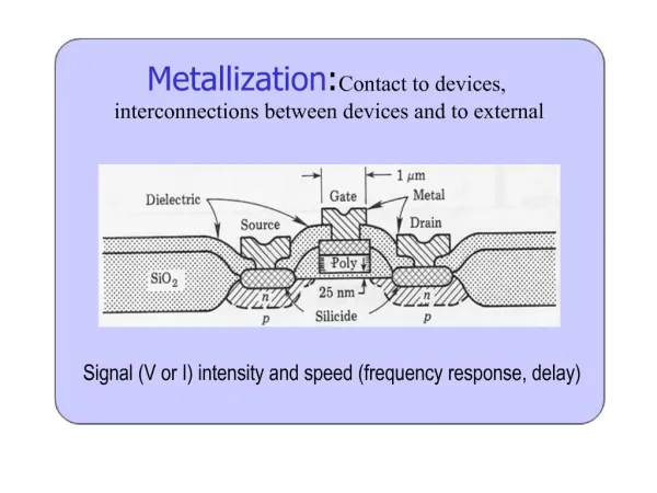
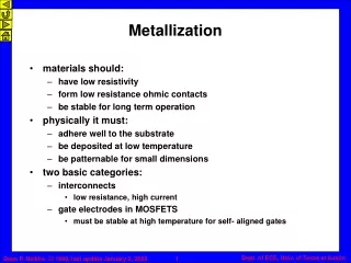
Metallization • materials should: • have low resistivity • form low resistance ohmic contacts • be stable for long term operation • physically it must: • adhere well to the substrate • be deposited at low temperature • be patternable for small dimensions • two basic categories: • interconnects • low resistance, high current • gate electrodes in MOSFETS • must be stable at high temperature for self- aligned gates
Materials for Interconnects and Contacts • aluminum • most common interconnect and contact material • 3 cm, 0.03 @ 1 m • excellent adherence to oxides • good ohmic contacts to Si • copper • primarily used as an interconnect material • 1.7 cm, ~0.02 @ 1 m • gold • very inert; adheres poorly • 2.5 cm, 0.025 @ 1 m • used mainly for GaAs interconnects
Materials for Interconnects and Contacts • polysilicon • used mainly for gate materials • ≥ 300 cm, @ 1m • high temperature stability • refractory Metals • chromium, palladium, tungsten • very high temperature stability • used mainly as reaction barriers • refractory Silicides • moderate resistivities • WSi2 70 cm • Pd2Si 30 cm • good high temperature stability • used with poly as gate metallization
nitride poly oxide silicon Self-Aligned silicide MOSFET SALICIDE process • oxidize sidewalls of poly • etch contact windows, strip nitride • deposit metal (Pt, Ti)
silicide metal silicide poly SALICIDE process • heat to drive reaction, form silicide • selective etch of unreacted metal • can also use cvd deposited oxide to form sidewall spacers
Rcontact = rc / contact area metal current flow lines insulator semiconductor Ohmic Contacts • general requirements • low contact resistance • specific contact resistivity rc (W•cm2) • non-injecting contact • should not damage substrate • basic techniques • form n+ - p+ wells in Si, then metallize • forms Schottky, but is dominated by tunneling currents for ND > 1019 cm-3 • p+ to n+ junction • forms symmetric tunnel junction with zero breakdown voltage • for Al to Si can use the Al as source for p+ doping • rc ~ 10-6 - 10-8W•cm2Æ 1mm2 contact ~ 100W - 1W resistance
Si “condensate” pit transport of Si insulator semiconductor ~1µm from Sze, 2nd, p. 408. Ohmic Contacts • major problem • Kirkendall effect • after 450˚C contact “forming” step • pits appear at Al/Si interface • after cooling silicon “boulders” are imbedded in the Al • junction “spiking” can occur if a shallow p-n junction is below the contact window • what causes this? • what about interdiffusion and solid solubility?
adapted from Campbell, p. 406. liquid only eutectic point two phase mix, l & s two solid phases Al - Si binary phase diagram • solid solubility of • Si in Al @ 450˚ C : 0.5 wt.% • Al in Si @ 450˚ C: 0.001 wt% • must satisfy solid solubility requirements for two dissimilar materials in contact • when Al contact is formed on Si there is a net dissolution of the silicon • large diffusion of Si along Al grain boundaries also occurs
Kirkendall Effects on Contacts • solutions • add 1 % Si to Al during deposition, along with Cu to prevent electromigration • use multilayer contact metallization: • adjacent to Si deposit • platinum silicide • 500 Å Pt + 665 Å Si consumed gives 990 Å PtSi • palladium silicide • 500 Å Pd + 500 Å Si consumed gives 720 Å Pd 2 Si • followed by 2000 Å TiW (20% Ti ) for adhesion, diffusion and intermetallic barrier • Al or Au interconnect metal
Intermetallic compounds at metal interface • "Purple Plague": • traditional bonding wire between IC and its package lead frame is gold • if a high temperature (~400˚C) step is used after bonding (e.g., to attach a metal package lid) open circuits result • aluminum and gold form the compounds • Au2Al: tan, brittle, poor conductor • AuAl2: purple, good conductor • to combine the two metallizations you could use diffusion/reaction barriers • deposition of Ti, Cr, Ta for adhesion • barrier of W or Mo • gold • barrier of Pt • barrier of Ti • aluminum
~5µm from Sze, 2nd, p. 410. Electromigration in Interconnects • transport of mass in metals due to momentum transfer from electrons when the conductor is subjected to very high current densities • typical current densities in IC’s 105 A / cm2 • 1 mA, 1 µm2Æ 105 A/cm2 • one of most significant failure modes in interconnects • mean time to failure depends on • current density j, temperature, material properties • n: between1 and 3, typically about 2 • Ea: activation energy, critically dependent on microstructure • grain size very important • electromigartion tends to • decrease for metals with higher melting points • decrease for metals with higher atomic number (mass)
adapted from Sze, 1st ed., p. 372. Electromigration in Interconnects • in aluminum films: • most migration along grain boundaries • control (increase) grain size by: • incorporate 0.5% - 4% Cu in film • control deposition conditions • in VLSI, linewidths may be small enough to form single crystal segments which reduce electromigration effects • new(er) problem: • stress induced voids in metal films
C. Wu, “Computer Chips Take a Leap Forward,” in Science News, vol. 152, 1997, pp. 196. L. Geppert, “Technology 1998, Analysis and Forcast: Solid State,” in IEEE Spectrum, vol. 35, 1998, pp. 23-28. Copper Interconnects • multi-level copper interconnects • reduce electrical resistance • reduces RC delay • smaller lines higher packing density fewer number of layers need for wiring reduced cost • improve electromigration resistance • smaller lines higher packing density fewer number of layers need for wiring reduced cost • issues • deposition usually via electroplating • seed layer required, usually via PVD or CVD • diffusion of copper • requires barrier layers: Ti/N, Ta/N • dry etch of copper is challenging • corrosion • cover sidewalls with TiN, other refractory, before copper deposition
Chemical-mechanical polish (CMP) • in multi- level interconnect planarization is limiting problem • CMP • lithography/etch to pattern metals • deposit dielectric • polish to planarize dielectric surface • deposit dielectric • etch contact openings (vias) , deposit via “plug” material, etch/polish as needed • repeat starting with deposition/patterning of next metal lines
Damascene process • deposit dielectric • etch “trenches” that are where you want metal lines • “line” trenches if necessary • blanket deposit metal • polish metal back to dielectric surface • deposit dielectric • open vias • deposit via plug material • repeat by depositing dielectric, etching trenches to be filled with metal • dual damascene process: use one layer of dielectric that has pattern for vias and metal lines
ref: R. W. Mann, L. A. Clevenger, P. D. Agnello, and F. R. White, “Salicides and local interconnections for high-performance VLSI applications,” IBM J. Res. Develop., vol. 39, pp. 403-417, 1995. Photo p. 414. Damascene/CMP example • dielectric layers have been etched away to reveal metal lines • SRAM cell • green: word lines, salicided poly • yellow: 1st global, Ti/Al(Cu)/Ti/TiN • pink: local (intra-cell), tungsten • grey: contact studs, tungsten
exposing radiation mask blank: transparent, mechanically rigid mask masking layer: opaque, patternable imaging system (low pass filter) photoresist film to be patterned substrate (with topography!) made soluble made insoluble Microlithography • Geometry Trends • Master Patterns: Mask technology • Pattern Transfer: Mask Aligner technology • Wafer Transfer Media: Photo resist technology NEGATIVE POSITIVE develop etch
Summary Slide • Metallization • Ohmic Contacts • Electromigration in Interconnects • Self-Aligned silicide MOSFET SALICIDE process • Chemical-mechanical polish (CMP) • next topic: lithography