Overview of the 8051 Microcontroller Family: Features, Pinouts, and Architecture
240 likes | 423 Vues
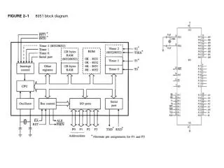
The 8051 microcontroller is a member of the MCS-51 family developed by Intel, recognized for its consistent design architecture across various models. This overview details its key specifications, including on-chip memory, timers, and function of each pin in its 40-pin package. The 8051 features four 8-bit I/O ports, a serial interface, 64K external code and data memory space, and a built-in Boolean processor. It also discusses the internal ROM and RAM, including registers, bit-addressable locations, and special function registers (SFRs), which enhance programming capabilities.

Overview of the 8051 Microcontroller Family: Features, Pinouts, and Architecture
E N D
Presentation Transcript
8051 Family The 8051 is just one of the MCS-51 family of microcontrollers developed by Intel. The design of each of the MCS-51 microcontrollers are more or less the same. The differences between each member of the family is the amount of on-chip memory and the number of timers, as detailed in the table below. Each chip also contains: four 8-bit input/output (I/0) ports , serial interface ,64K external code memory space 64K external data memory space , Boolean processor ,210 bit-addressable locations 4us multiply/divide, two 16 bit timers
FIGURE 2–2 8051 pinouts The diagram above shows the 8051 pinout. The chip is a 40-pin package. Port 0 - pins 32 to 39 make up the 8-bit I/O port 0. However, if external memory is used, these lines are used as a multiplexed address and data bus. Port 1 - pins 1 to 8 make up the 8-bit I/O port 1. Port 2 - pins 21 to 28 make up the 8-bit I/O port 2. However, if external memory is used, these lines make up the high-byte of the external address (A8 to A15). Port 3 - pins 10 to 17 make up the 8-bit I/O port 3. However, each of these eight pins also has an alternate function, as detailed in the table below. ( next slide)
RST - the reset input is on pin 9. This pin is used for resetting the 8051 (ie; loading the PC with the correct startup value). EA-bar - the external access, on pin 31, is used for enabling or disabling the on-chip ROM. When tied high (5V), the 8051 executes instructions in internal ROM when executing in the lower 4K (8K for the 8052) of memory. If tied low the 8051 will always execute instructions in external memory. The 8031 and 8032 should always have pin 31 tied low as there is no internal code memory. ALE - the address latch enable is on pin 30. The ALE is used for latching the low byte of the address into an external register. We will deal with this at a later date. PSEN-bar - the program store enable is an output signal on pin 29. This signal is used for fetching instructions from external code memory. We will also deal with this at a later date.
FIGURE 2–3 Driving the 8051 from a TTL oscillator Nominal crystal frequency 12MHz. Power Connection +5V
FIGURE 2–5 Relationship between oscillator clock cycles, states, and the machine cycle 8051 requires two clock cycles to perform a single discrete operation. Which is either fetching an instruction, decoding or executing it. This duration of two clock cycles is also called a state (S). In order to fully process an information (generally), 8051 would require six such states, or 12 clock cycles. Since it would have to first fetch and decode the instruction before it goes to execute it. This duration of six state also known as machine cycle. ( Of course, more complex instructions would require more than one machine cycle to be carried out. Typically, 8051’s on chip oscillator, is driven by a 12 MHz crystal, period of one clock cycle = 83.33 ns. One machine cycle consists of 12 such clock pulses, hence its duration is 83.33ns* 12 = 1 micro sec.
FIGURE 2–7 Summary of the 8051 on chip data memory Internal ROM The 8051 has 4K (4096 locations) of on-chip ROM. This is used for storing the system program. 2^12 = 4096, therefore the internal ROM address bus is 12 bits wide and internal ROM locations go from 000H to FFFH. Internal RAM There are 256 bytes of internal RAM on the 8051. 28 = 256, therefore the internal RAM address bus is 8 bits wide and internal RAM locations go from 00H to FFH. The first 128 locations (00H to 7FH) of internal RAM are used by the programmer for storing data while the second 128 locations (80H to FFH) are the Special Function Registers (SFRs) which we will deal with later.
Register Banks There are four register banks from 00H to 1FH. On power-up, registers R0 to R7 are located at 00H to 07H. However, this can be changed so that the register set points to any of the other three banks (if you change to Bank 2, for example, R0 to R7 is now located at 10H to 17H). Bit-addressable Locations The 8051 contains 210 bit-addressable locations of which 128 are at locations 20H to 2FH while the rest are in the SFRs. Each of the 128 bits from 20H to 2FH have a unique number (address) attached to them, as shown in the table above. The 8051 instruction set allows you to set or reset any single bit in this section of RAM.With the general purpose RAM from 30H to 7FH and the register banks from 00H to 1FH, you may only read or write a full byte (8 bits) at these locations.However, with bit-addressable RAM (20H to 2FH) you can read or write any single bit in this region by using the unique address for that bit. We will later see that this is a very powerful feature. Special Function Registers (SFRs) Locations 80H to FFH contain the special function registers. As you can see from the diagram , not all locations are used by the 8051 (eleven locations are blank). These extra locations are used by other family members (8052, etc.) for the extra features these microcontrollers possess. Also note that not all SFRs are bit-addressable. Those that are have a unique address for each bit. We will deal with each of the SFRs as we progress through the course, but for the moment you should take note of the accumulator (ACC) at address E0H and the four port registers at addresses 80H for P0, 90h for P1, A0 for P2 and B0 for P3. We will later see how easy this makes ready from and writing to any of the four ports. Note: registers & I/O ports are memory mapped, accessible like any other memory location.
The Missing Registers The two registers not shown in the table above are the instruction register and the program counter. These two very important registers are not placed in RAM because it is not necessary to make them directly accessible to the programmer. The instruction register gets its data from the execution cycle while the program counter is manipulated by the operation of these instructions. The Special Function Registers (SFRs) The SFRs are in locations 80H to FFH of the on-chip RAM. In the 8051 not all locations are used. These extra locations are used by other family members (8052, etc.) for the extra features these microcontrollers possess. As you can see, some of the SFRs are bit addressable, including the four ports P0, P1, P2 and P3. Program Status Word (PSW) The PSW is at location D0H and is bit addressable. The table below describes the function of each bit.
Carry Flag : The carry flag has two functions. Firstly, it is used as the carry-out in 8-bit addition/subtraction. For example, if the accumulator contains FDH and we add 3 to the contents of the accumulator (ADD A, #3), the accumulator will then contain zero and the carry flag will be set. It is also set if a subtraction causes a borrow into bit 7. In other words, if a number is subtracted from another number smaller than it, the carry flag will be set. For example, if A contains 3DH and R3 contains 4BH, the instruction SUBB A, R3 will result in the carry bit being set (4BH is greater than 3DH). The carry flag is also used during Boolean operations. For example, we could AND the contents of bit 3DH with the carry flag, the result being placed in the carry flag - ANL C, 3DH Register Bank Select Bits Bits 3 and 4 of the PSW are used for selecting the register bank. Since there are four register banks, two bits are required for selecting a bank, as detailed below. For example, if we wished to activate register bank 3 we would use the following instructions - SETB RS1SETB RS0 If we then moved the contents of R4 to the accumulator (MOV A, R4) we would be moving the data from location 1CH to A.
Parity Bit • The parity bit is automatically set or cleared every machine cycle to ensure even parity with the accumulator. The number of 1-bits in the accumulator plus the parity bit is always even. In other words, if the number of 1s in the accumulator is odd then the parity bit is set to make the overall number of bits even. If the number of 1s in the accumulator is even then the parity bit is cleared to make the overall number of bits even. For example, if the accumulator holds the number 05H, this is 0000 0101 in binary => the accumulator has an even number of 1s, therefore the parity bit is cleared. If the accumulator holds the number F2H, this is 1111 0010 => the accumulator has an odd number of 1s, therefore the parity bit is set to make the overall number of 1s even. As we shall see later in the course, the parity bit is most often used for detecting errors in transmitted data. • B Register • The B register is used together with the accumulator for multiply and divide operations. • The MUL AB instruction multiplies the values in A and B and stores the low-byte of the result in A and the high-byte in B. • For example, if the accumulator contains F5H and the B register contains 02H, the result of MUL AB will be A = EAH and B = 01H. • The DIV AB instruction divides A by B leaving the integer result in A and the remainder by B. • For example, if the accumulator contains 07H and the B register contains 02H, the result of DIV AB will be A = 03H and B = 01H. • The B register is also bit-addressable.
Stack Pointer The stack pointer (SP) is an 8-bit register at location 81H. A stack is used for temporarily storing data. It operates on the basis of last in first out (LIFO). Putting data onto the stack is called "pushing onto the stack" while taking data off the stack is called "popping the stack." The stack pointer contains the address of the item currently on top of the stack. On power-up or reset the SP is set to 07H. When pushing data onto the stack, the SP is first increased by one and the data is then placed in the location pointed to by the SP. When popping the stack, the data is taken off the stack and the SP is then decreased by one. Since reset initializes the SP to 07H, the first item pushed onto the stack is stored at 08H (remember, the SP is incremented first, then the item is placed on the stack). However, if the programmer wishes to use the register banks 1 to 3, which start at address 08H, he/she must move the stack to another part of memory. The general purpose RAM starting at address 30H is a good spot to place the stack. To do so we need to change the contents of the SP. MOV SP, #2FH. Now, the first item to be pushed onto the stack will be stored at 30H PORT REGISTERS SERIAL PORT REGISTERS INTERRUPT REGISTERS POWER CONTROL REGISTERS DATA POINTER ( DPTR )
FIGURE 2–8 Multiplexing the address bus (low-byte) and data bus External memory
FIGURE 2–16 Two circuits for system reset. (a) Manual reset (b) Power-on reset.