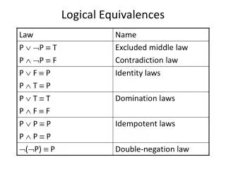
Logical Functions
Logical Functions. Circuits using NMOS and PMOS enhancement mode FETs. Rules. Each logical gate has its own load resistor or saturated load. Each ‘bar’ in the function should be implemented as a separate logical gate.

Logical Functions
E N D
Presentation Transcript
Logical Functions Circuits using NMOS and PMOS enhancement mode FETs
Rules • Each logical gate has its own load resistoror saturated load. • Each ‘bar’ in the function should be implemented as a separate logical gate. • If the function does not have a bar over the entire Boolean expression, then the final gate is an inverter.
NMOS Logic • Determine how many bars there are in the circuit. The sum of the bars is equal to the number of individual logical gates that will be needed to implement the function. • If there is a missing bar over the entire Boolean function, draw two bars over the entire function. • Working from the smallest grouping to the complete Boolean function, begin drawing logical gates.
NMOS Logical Gate Layout • Logical ANDs are NMOSFETs in series and logical ORs are NMOSFETs in parallel. • An individual variable with a bar over it means that the unbarred variable is an input to an inverter. • Place load above and the NMOS devices below the output terminal. • If the logical expression implemented in the grouping of FETs is part of a larger expression, the output terminal should be connected to the gate of a FET in the next logical gate.
PMOS Logical Gate Layout • If you have implemented the circuit as an NMOS logical circuit, then you can redraw it using PMOSFETs. • Logical ANDs are PMOSFETs in parallel and logical ORs are PMOSFETs in series. • Change any parallel groups of NMOSFETs to groups of PMOSFETs in series. • Change any series groups of NMOSFETs to groups of PMOSFETs in parallel. • Place load below and the PMOS devices above the output terminal. • As with the NMOS logic: If the logical expression implemented in the grouping of FETs is part of a larger expression, the output terminal should be connected to the gate of a FET in the next logical gate.
Directly Implementing PMOS Logic • Use DeMorgan’s Theorem to redistribute the bars in the logical expression. • DeMorgan’s Theorem can be applied to small groupings of variables that are barred within the Boolean Expression. • Or, the output of the logical function that implements the small expression should be tied to a PMOS inverter before implementing the next larger grouping of variable.
PMOS Logic: DeMorgan’s Theorem • Variables that are barred should be connected directly to the gate of a PMOSFET. • Variables that are missing a bar should be connected to a PMOSFET inverter. • Logical ANDs are PMOSFETs in series and logical ORs are PMOSFETs in parallel.
NMOS • When either MA or MB is turned on, Vo is pulled down towards ground. • When both MA and MB are off, ML pulls Vo up to VDD. • When both MA and MB are turned on, Vo is pulled down towards ground. • When either MA and MB or off, ML pulls Vo up to VDD.
PMOS • When both MA and MB is turned on, Vo is pulled up to VDD. • When either MA or MB are off, ML pulls Vo down towards 0V. • When either MA or MB is turned on, Vo is pulled up to VDD. • When both MA and MB are off, ML pulls Vodown towards 0V.
Writing a Boolean Function • NMOS circuit • Inputs to each gate are written as is. • All paths to ground are OR’ed together. • All FETs in series along the path are AND’ed together. • Place a bar over the entire function implemented in the circuit. • PMOS circuit • Inputs to each gate are written with a bar over them. • All paths to VDD are OR’ed together. • All FETs in series along the path are AND’ed together. • Do not place bar over the entire function implemented in the circuit.