a) b)
V G. N poly. t poly. t ox. V S. Na Silicon layer t s. V D. N poly. V G. TU Munchen MOS-AK/ESSDERC/ESSCIRC Workshop Sept. 14, 2007.

a) b)
E N D
Presentation Transcript
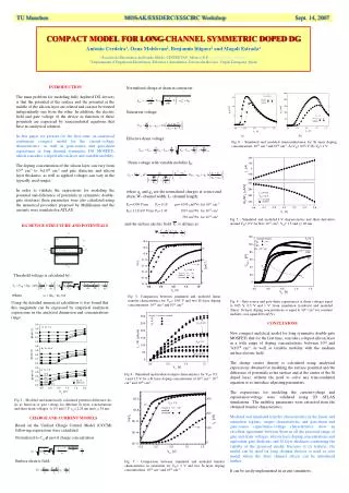
VG Npoly tpoly tox VS Na Silicon layer ts VD Npoly VG TU Munchen MOS-AK/ESSDERC/ESSCIRC Workshop Sept. 14, 2007 COMPACT MODEL FOR LONG-CHANNEL SYMMETRIC DOPED DGAntonio Cerdeira1, Oana Moldovan2, Benjamín Iñiguez2 and Magali Estrada11 Sección de Electrónica del Estado Sólido, CINVESTAV, México D.F., cerdeira@cinvestav.mx2 Departament d´Enginyeria Electrònica, Elèctrica i Automàtica, Universitat Rovira i Virgili,Tarragona, Spain INTRODUCTION The main problem for modeling fully depleted DG devices is that the potential at the surface and the potential at the middle of the silicon layer are related and can not be treated independently one from the other. In addition, the electric field and gate voltage of the device as function of these potentials are expressed by transcendental equations that have no analytical solution. In this paper we present for the first time, an analytical continuous compact model for the current-voltage characteristics, as well as gate-source and gate-drain capacitance in long channel symmetric DG MOSFETs which considers a doped silicon layer and variable mobility. The doping concentration of the silicon layer can vary from 1014 cm-3 to 3x1018 cm-3 and gate dielectric and silicon layer thickness, as well as applied voltages can vary in the typically used ranges. In order to validate the expressions for modeling the potential and difference of potentials in symmetric double-gate structures these parameters were also calculated using the numerical procedure proposed by Mallikarjun and the currents were simulated in ATLAS. Normalized charge at drain in saturation: Saturation voltage: a) b) Fig 6 - Simulated and modeled transconductance for Si layer doping concentrations: 1015 cm-3 and 1018 cm-3. A) VD= 0.05 V; B) VD= 1 V. Effective drain voltage: Drain voltage with variable mobility ID: where qs and qd are the normalized charges at source and drain; W- channel width; L- channel length; E1= 6300 V/cm P1= 0.19 o= 1043 cm2/Vs for 1015 cm-3 E2= 1.12x10⁶ V/cm P2= 1.45 1015 cm2/Vs for 1017 cm-3 793 cm2/Vs for 1015 cm-3 Fig 7 - Simulated and modeled I-V characteristics and their derivative around VD= 0 V for Na= 1017 cm-3; VG= 1.5 and ts= 20 nm. and the surface electric field is defines as: DG DEVICE STRUCTURE AND POTENTIALS Threshold voltage is calculated by: where Fig 3- Comparison between simulated and modeled linear transfer characteristics for VD= 0.05 V and two Si layer doping concentrations: 1015 cm-3 and 1018 cm-3. Fig. 8 - Gate-source and gate-drain capacitances at drain voltages equal to 0.05 V, 0.5 V and 1 V: from simulation (symbols) and modeled (lines). Si layer doping concentrations is equal to 1016 cm-3 for constant mobility case equal 400 cm2/Vs. Using the detailed numerical calculation it was found that this magnitude can be expressed by empirical analytical expressions in the analyzed dimension and concentrations range. CONCLUSIONS New compact analytical model for long symmetric double-gate MOSFETs that for the first time, considers a doped silicon layer in a wide range of doping concentrations, between 1014 and 3x1018 cm-3, as well as variable mobility with the medium surface electric field. The charge carrier density is calculated using analytical expressions obtained for modeling the surface potential and the difference of potentials at the surface and at the center of the Si doped layer, without the need to solve any transcendental equation or to introduce adjusting parameters. The expressions for modeling the current-voltage and capacitance-voltage were validated using 2D ATLAS simulations. The mobility parameters were extracted from the obtained transfer characteristics. Modeled and simulated transfer characteristics in the linear and saturation regions, output characteristics and gate-drain and gate-source capacitance-voltage characteristics show an excellent agreement between them in all the practical range of gate and drain voltages, silicon layer doping concentrations and equivalent gate dielectric and Si layer thickness confirming the validity of the proposed model.Because of its features, the model can be used for long channel devices or used as core model where the short channel effects can be introduced further. It can be easily implemented in circuit simulators. Fig 4 - Simulated and modeled output characteristics for VG= 0.5, 1 and 1.5 V for a Si layer doping concentration of 1015 cm-3; 1017 cm-3 and 1018 cm-3. Fig 2 - Modeled and numerically calculated potential difference s-o as function of gate voltage for different Si layer concentrations and three drain voltages: 0, 0.5 and 1 V. tox= 2.24 nm and ts= 34 nm. CHARGE AND CURRENT MODELS Based on the Unified Charge Control Model (UCCM) following expressions were calculated: Normalized to Coxt movil charge concentration Surface electric field: Fig. 5 - Comparison between simulated and modeled transfer characteristics in saturation for VD= 1 V and two Si layer doping concentrations: 1015 cm-3 and 1018 cm-3.

