Download
1 / 18
210 likes | 416 Vues
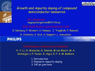
M.T. Borgström magnus.borgstrom@ftf.lth.se. Growth and impurity doping of compound semiconductor nanowires. Solid State Physics, Lund University, Lund E. Norberg, P. Wickert, H. Nilsson, J. Trägårdh, P. Ramvall, G. Statkute, K. Dick, K. Deppert, L. Samuelson

E N D
M.T. Borgström magnus.borgstrom@ftf.lth.se Growth and impurity doping of compound semiconductor nanowires Solid State Physics, Lund University, Lund E. Norberg, P. Wickert, H. Nilsson, J. Trägårdh, P. Ramvall, G. Statkute, K. Dick, K. Deppert, L. Samuelson Philips Research laboratories, Eindhoven H -Y. Li, O. Wunnicke, G. Immink, M van Weert, M. A. Verheijen, L-F. Feiner, R. Algra, E. P. A. M. Bakkers 1. Introduction 2. Nanowire impurity doping 3. InP pn junctions
Energy (transformed from one form to another) • 50times increase in energy consumption since pre industrial era (15 terawatt-years per year) • US, 300 million, 5 % of world population > 21 % world energy consumption • India, 1000 million, 16 % worlds population 3.4 % world energy consumption Mrs Bulletin, 2008. 33
Power to the people(renewable energy) Off-Grid solar cells: Nasa ISS Mrs Bulletin, 2008. 33
liquid Au-III eutect vapor Metal particle III-V nanowire time VLS (Vapor-Liquid-Solid) Crystal Growth Small lateral dimensions: Elastic strain relaxation via surface Single nucleation event (III/V on Si) Nanowires Wagner and Ellis, APL, 1964
Impurity doping in nanowires • Particle assisted growth: • Low temperature (400-500ºC) MOVPE 600-700ºC • Via catalyst particle ? • Complex growth dynamics • [111] growth direction • crystal structure • Large surface/bulk ratio: Surface states • Characterisation: • Chemically (EDX) • Electrically (Field effect) • Optically (PL) • Atom probe
Deliberate NW doping in literature • Hiruma (GaAs p-n junction, APL 1992) • Meyyappan (p and n-type ZnO, Nano letters 2004) • H-M. Kim (GaN p-n junction, Nano letters 2004) • Appenzeller (Ge p-n junction, Nano letters 2006) • Bakkers (p and n –type InP, InAs, Nano letters 2007) • Lieber (p and n-type InP, GaN, Si p-n junction, dopant modulation) Lieber, Nano Letters 2008
Evaluate doping – nw-FET • Drude model, nq • Carrier concentration, n = doping concentration • Mobility (µ) extracted from gate-sweep measurements • Conductivity (σ) extracted from I-V n-type
TESn for n-doping (Sn:InP ionization energy 5.9 meV) • Gate voltage dependent action - n-type • transconductance + IV (ohmic contacts) • threshold voltage (non ohmic contacts)
TESn for n-doping (Sn:InP ionization energy 5.9 meV) • Gate voltage dependent action - n-type • transconductance + IV (ohmic contacts) • threshold voltage (non ohmic contacts) • TESn: excellent n type InP dopant precursor
Dimethylzinc for p-doping(Zn:InP ionization energy 35 meV) • DMZn enhances the nanowire growth rate and suppresses side wall growth • Nucleation problems for high dopant precursor molar fraction XDMZn=1e-6, 20min XDMZn=1e-5, 20min XDMZn=5e-5, 20min
Evaluate doping – Results DMZn • p -type PL behaviour • P-type gate voltage dependent behaviour • Normally turned off at zero gate voltage: low doping • Incomplete DMZn pyrolysis Van Weert el al, APL, 2006
DiEthylZinc for p doping • DEZn more effective dopant precursor than DMZn • InP :DEZn Vth=10V (~1018 cm-3) Minot et al, Nano Letters, 2007
n+p junctions • XTESn=1E-5, XDMZn=5.5 E-5 • ND=6E18 cm-3, NA= xE17 • 80 nm Au catalyst p-InP n-InP n- InP (111)B order is important
n+p junction- IV • pn junction behaviour • Reverse breakdown voltage about 20V • Ideality factor around 3 Do they shine?
Electroluminescence • Light emitting diode • Quantum efficiency ~10-5 at 300K
Photo current measurements • Voc (707 W/cm2) = 0.97V
Summary InP • TESn – n type dopant with excellent controllability • H2S – n type dopant (high doping levels shown) • DMZn- affects nanowire growth rate - low doping levels • DEZn – versatile p-dopant precursor • InAs/InP Core-Shell modulation doping • pn-junctions