Interactive Micro Braille Technology for Enhanced Accessibility
µBITS is a groundbreaking project designed to empower the blind by integrating a micro interactive touch screen with a unique pin bed capable of displaying scrolling Braille and simple images. This compact and portable device supports various character sets and provides flexibility through USB and PS/2 interfaces. The system also includes integrated keyboard support, ensuring seamless interaction with computers and the internet. Our innovative design prioritizes user safety and compliance with FCC standards, making it an essential tool for improved accessibility and communication.

Interactive Micro Braille Technology for Enhanced Accessibility
E N D
Presentation Transcript
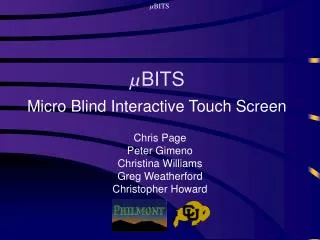
µBITS Micro Blind Interactive Touch Screen Chris Page Peter Gimeno Christina Williams Greg Weatherford Christopher Howard
Purpose • To give the blind the capability to interface with a computer and the internet. • To create a pin bed that can display scrolling, Braille characters, ASCII characters, a few Japanese characters and simple monochromatic images. • To create a pin bed that is compact and more portable than current Braille books. • With a flexible I/O interface capable of USB and PS/2
Presentation Overview • Requirements and Standards • Block Diagram • Digital Design Process • Software • Analog Design Process • Interface between D/A • Schedule/Division of labor • Cost • Questions, Comments?
Product Overview • A three dimensional display board. • Designed for use by the blind. • Capable outputting multiple character sets • Flexible I/O interface • Integrated Keyboard Support (USB or PS/2) • Software designed to support up to a 320x240x8 pin display. • Compact
Operation at standard room temperatures. Safe for end user operation. Compliant with FCC standards. Safe for pacemaker users. Initial Requirements – Environmental Standards
Initial Requirements - Performance Standards • CPU Capable of image/video decoding. • 512Kb of frame backing/character lookup memory. (Was 2Mb) • 3Mb of CPU memory. (Was 4Mb)
Initial Requirements – Interface Standards • P/S 2 keyboard input • Pin Grid Output • 2 General purpose I/O inputs • Capable of supporting USB, IDE, Digital Cameras, serial, and many other popular input methods.
Block Diagram Future I/O Expansion P/S 2 Input FPGA Display Driver I/O Controller Analog Display Driver Memory 512Kb SRAM Frame Buffer and Character Lookup Table Pin Grid Processor CY7C67200 50 MHz GCC programmable Power supply DC –DC converters Memory 3Mb SRAM Future Expansion
Nesting Diagram CPU Board (CIB) FPGA Board (PGGU) Pin Grid Driver Board (PGD) Digital Power Supply PGGU VRAM Board (VRAM) Analog Power Supply
Board Features • IDE/GPIO interface • Direct RAM communication with FPGA • Serial Debug Interface • LED Status Indicators • Overcurrent and Undervoltage CPU Protection • HSSI • 2 independent USB data and power busses • Prominent Reset Button
Digital Progress • Determined Specification Details • Part selection • Schematic Capture • Schematic Review • Layout • Board Manufacturing • Board Electrical Test • Board Population • Board Operational Testing • Software
Proposed Software Diagram SRAM CPU FPGA HDL SRAM Receiver SRAM Driver Encoder Image Processing VRAM Driver Display Driver Font LUT Decoder USB Driver (serial) USB Driver (HID) PS/2 Driver Braille LUT Data (computer) USB HID Device (Keyboard) PS/2 Keyboard Display
SRAM/FPGA Data Transfer • 128 addressable bytes • Byte 0 is command byte • Byte 127 is status byte • Bytes 120-126 are pin grid display mode registers. • Bytes 1-10 are Data bytes
Current Digital Issues • Communication Protocols • HDL Way Behind Schedule • NO PROJECT SOFTWARE HAS BEEN WRITTEN YET! • Data Representation • Group Communication
Analog over view • Progress • Design • Prototype Design Details • Ideas that didn’t work • Problems/solutions • Current problems • Future Goals
Analog Progress • Tested pin elevation techniques • Designed three character Braille board • Cut Braille board on Laser cutter in ITLL • Chose and modified power supply for Braille board • Designed schematic for Braille board • Tested Design • Begin building three character Braille board
Failed Idea: High-Z DeMUX Decoder • Requires a high refresh rate for even small designs • Solenoids are limited to roughly a 30 Hz refresh rate • For 100 pins, this would take over 3 seconds to refresh each pin • Since the pin is only active for this brief refresh period, gravity does becomes an issue Outputs FPGA Decoder 1 Z Decoder Z 0 Z
Promising Design: M&M (MUX Memory) Outputs • More complex then High-Z DeMUX design • Memory will allow pins to remain elevated • Eliminates possible problems with surrounding pins FPGA Clock DEMUX Memory Reset Current Driver Pin Grid
Analog Design (LPBB): Actual Pin Board Design • (From PDR) We are looking to modulize each 2x3 section. • We did not modulize because we are dealing with a low amount of characters (only 2-3 char.) • (From PDR) The pins will meet Braille specifications. • We did not meet the Braille specifications but we accomplished to be off only be approx. 0.05” between characters. Pin 6 - Capitalization 0.200” Pins 2, 3, 4 – Full Character 0.02” to 0.05” 0.20” Distance between each Braille module = 0.6”
Analog Design : First Prototype • Will be a 2x3 board. (one Braille character) • Need to test board dimensions. • Will use magnetic elevation (ME). • Need to know wrapping to current ratio. • Size of pins needed. • Will use one of the pin addressing designs. • Depends on if High Z MUX will perform as expected within a reasonable cost. • Will not be connected to FPGA, will simulate FPGA output.
Analog Design : Prototype Checklist • Pin has to elevate to correct height. • Record winding to current ration for correct height. • Pin has to stay elevated at correct height for specific amount of time. • Touching our display will not cause harm to the person. • Measured operating characteristics of each solenoid • Up to 12V • 0.3 to 1 Amp • 30 Hz or less
Analog Design : Current Design • Can display 5 Braille characters • Uses magnetic elevation (ME) • Due to the size of the solenoids, a multi level design was used • Uses Direct Pin Addressing • Has yet to be connected to the FPGA • Can still be operated manually
Analog ComponentsFor the 3 character Braille board • Power supply, can supply up to 20 A @ 5V • Voltage Regulator • 560 1/4 Watt resistor • 1.1K 1/4 Watt resistor • 2N3055 Power transistor • 2N2222A NPN transistor 600mA @6V DC continuously • 18 Solenoid actuators. 10 ohms, .3A @2.3V continuously • Plastic board to hold the assembly, 4 layers. • 2 of 0.13” bolts to hold assembly together. • 10 of 0.13” nuts to hold the levels in place on the assembly • 18 of 0.025” sewing pins with flat tops. • 18 1K 1/8 watt resistors to current limit the FPGA
Voltage regulator, Single pinfor the 3 Character Braille board
Analog Design : Issues that have been Addressed • Layout Board • Record list of manufactures and stores needed. • Solenoids will be purchased rather then made • Begin tests of layout board • Looked specifically at: • Pin addressing • Pin Board Layouts / Designs • People contacted for input or design issues • Lucy Pao – CU • Gagandeep Lamba – CU
Analog Design : Issues to be Addressed • Programming the FPGA • Learning Verilog and programming a PS/2 interface • Building the ‘Blow Out’ Circuitry between the FPGA and the Pin Board • Safety precaution to prevent damage to FPGA I/O ports • Practical 3D designs
Analog Ideas that didn’t work • Using a capacitor to make the actuator have more current for the first ms. The time period is too long, the cap would have needed to be too big. • Magnetic pin elevation • Memory Metal pin elevation • Bimetallic pin elevation • Bobbin and drill for wrapping coils.
Future Goals • Interface three character Braille board to the Ps/2 keyboard • Test three more possible methods of 3-D pin elevation • Magnetic pins with Aluminum collars • Linear motors • Drop pins through coils. • Choose elevation method then design 100 pin board. • Purchase parts for 100 pin board • Build 100 pin board • Interface 100 pin board to CPU board
Analog Design : Next Steps (Prototype and Beyond) • Layout Board • Record list of manufactures and stores needed. • Wrapping solinoids. • Begin tests of layout board • Looking specificly at: • Scrolling • Pin addressing • Current Contacts to work with us • Lisa Pao - CU • NIST Researchs of Tactile Board • - • -
Interface between Digital and Analog • Progress • Ideas • Future Goals
Interface progress • Tested Mux matrix idea (did not work) • Learning Verilog to program firm ware for interface.(in progress) • Come up with possible design
Analog Design : Ideas for Implementation • Pin Addressing • High-Z MUX Decoder • Not very compatible with our design • Direct Pin Addressing
Serial to Parallel conversion • Accepts serial data from one I/O port on the FPGA which would then be used to send the correct voltage to multiple pins. • We would still need many S to P chips to address all the pins in the 100 pin bed.
Interface Future Goals • Select components for S to P idea • Build S to P prototype and test it. • Assemble final S to P interface for 100 pin bed.
Cost Estimate • FPGA development board: $175 • Computer PCB: $350 • PCB components $300.00 • Three character Braille pin bed $30.00 • 100 pin bed $200.00 • Digital-Analog Components: $50

