Download
1 / 1
10 likes | 111 Vues
Explore the impact of spatial distribution on ZnO:Al and ZnO:Sc films to optimize properties for thin-film solar cells and optoelectronic devices. Investigate sputtering effects on film properties, including composition, lattice stress, and crystallite size.

E N D
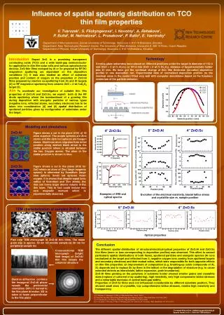
Influence of spatial sputterig distribution on TCO thin film properties V. Tvarozek1, S. Flickyngerova1, I. Novotny1, A. Rehakova1, P. Sutta2, M.Netrvalova2, L. Prusakova2, P. Ballo3, E. Vavrinsky1 1Department of Microelectronics, Slovak University of Technology, Ilkovicova 3, 812 19 Bratislava, Slovakia 2Department New Technologies Research Center, The University of West Bohemia, Univerzitni 8, 306 14 Plzen, Czech Republic 3Department of Physics, Slovak University of Technology, Ilkovicova 3, 812 19 Bratislava, Slovakia Technology IntroductionDoped ZnO is a promising transparent conducting oxide (TCO) and a wide band-gap semiconductor for application in thin film solar cells and various optoelectronic devices. ZnO thin films codoped by Al or Sc prepared by RF/DC magnetron sputtering are dependent on the deposition conditions [1]. It was also studied an effect of substrate position and content of oxygen on the properties of ZnO:Al films prepared by reactive co-sputtering from Zn and Al targets [2] or RF magnetron sputtering from ceramic ZnO + 2 wt.%Al2O3 target [3]. AimTo accelerate our investigation of suitable thin film properties of ZnO:Al and ZnO:Sc, we exploit both (i) the RF diode sputtering where the bombardment of a growing film during deposition with energetic particles of various types (negative ions, reflected atoms, secondary electrons) has to be taken into consideration [4] and (ii) spatial distribution of sputtered particles given by configuration of substrates under the target. Corning glass substrates were placed on different positions under the target in diameter of 152.4 mm (ZnO + 2 wt.% Al2O3) or 101.6 mm (ZnO + 2 wt.% Sc2O3), distance of target-substrate holder was 40 mm. We have got the continual change of thin film thickness (so-called deposition profile) in one deposition run. Experimental data of normalized deposition profiles (to the maximal value in the center) fitted very well with computer simulations based on the Knudsen cosine law of the particle emission. 6’’ ZnO:Al 4’’ ZnO:Sc 4” ZnO:Sc Modeling and simulations ZnO:Al Figure shows a cut in the plane (010) of 32 atom supercel. The purple spheres are Zinc atoms and the dark red spheres are Oxygen atoms.Aluminum atom migrates from initial position along dashed black arrow to the stable position where is situated between the two Oxygen atoms. The atom in the stable position is shown in blue. ZnO:Sc Figureshows a cut in the plane (010) for ZnO where an atom of Zinc (large magenta sphere) is alternated by Scandium (large blue sphere). Small red spheres mean oxygen. It is shown that despite equal ionic radius of Scandium and Zinc atoms, the first one forms larger atomic volume in the thin layer. This in fact could induce non zero magnetic moment which is experimentally observed. Examples of XRD and optical spectra Evolution of the electrical resistivity, biaxial lattice stress and crystallite size vs. sample position 6” ZnO:Al 4” ZnO:Sc TEM characterization of samples ZnO:Al (a) (b) Optical properties Plan view TEM micrograph of ZnO:Al thin films. The mean grain size is approx. 50 nm for middle sample (a) 20 nm for peripheral sample (b) Conclusion The different spatial distribution of structural/electrical/optical properties of ZnO:Al and ZnO:Sc thin films (more or less corresponding to deposition profiles) was observed. This effect is caused particularly spatial distributions of both fluxes, sputtered particles and energetic species (Ar ions neutralized at the target and reflected from it, negative oxygen ions coming from sputtered targets and secondary electrons) and their mutual ratios, which were responsible for both opposite effects on thin film properties: an improvement of composition (e.g. breaking-up oxide compounds of Al, Sc dopands and to replace Zn by them in the lattice) or the degradation of structure (e.g. to cause extended defects as intersticials, lattice expansion, grain boundaries). ZnO:Al films growing on the periphery of substrate holder showed smaller grains and crystallite sizes (regions of coherent x-ray scattering), high resistivity, very high compressive lattice stresses and a remarkable decrease of optical band-gap widths. Properties of ZnO:Sc films were not influenced considerable by different substrate position. They showed small sizes of crystallite, low comprehensive lattice stresses, relative high resistivity and transparency. Cross-sectional TEM micrograph (bright field image) of ZnO:Al thin film reveals the columnar structure Electron diffraction confirms the hexagonal ZnO:Al phase reveals the preferential orientation (001) in normal to the film plane direction. ED is taken at beam perpendicular to the film plane [1] T. Minami, T. Yamamoto, T. Miyata, Thin Solid Films 366 63 (2000) [2] Jing-Chie Lin, Kun-Cheng Peng, Hsueh-Lung Liao, Sheng-Long Lee, Thin Solid Films 516 5349 (2007) [3] F. Couzinie-Devy, N. Baaeau, J. Kessler, Thin Solid Films 516 7094 (2008) [4] V. Tvarozek, I. Novotny, P. Sutta, S. Flickyngerova, K. Schtereva, E. Vavrinsky, Thin Solid Films 515 8756 (2007) Corresponding author: vladimir.tvarozek@stuba.sk Special thanks to Dr. I. Vavra for TEM analyses