Download
1 / 59
620 likes | 906 Vues
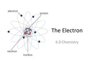
FIAP Jean Monnet-Institut de physique du globe, Paris, October 21-27, 2007. Castaing’s electron probe microanalyzer (electron microprobe) Michel Fialin Service CAMPARIS Campus universitaire Jussieu, Paris fialin@ccr.jussieu.fr. The electron microprobe. History

E N D
FIAP Jean Monnet-Institut de physique du globe, Paris, October 21-27, 2007 Castaing’s electron probe microanalyzer (electron microprobe) Michel Fialin Service CAMPARIS Campus universitaire Jussieu, Paris fialin@ccr.jussieu.fr
The electron microprobe History -> 1895 discovery of X-rays (WilhelmConrad Röntgen) -> 1909 observation of « characteristic » X-rays by electron bombardment of pure elements (Charles G. Barkla, C.A. Sadler) -> 1912 diffraction of X-rays by a systematic crystal (Wave nature of X-rays) (Maxvon Laue). -> 1913 basis of all X-ray spectrometry established (first X-ray spectrum produced, X-rays produce ionization, first X-ray detector)(William Henry and his son William Lawrence Bragg) -> 1913 relationship between the atomic number of an element and the energy of the X-rays produced from it (Moseley’s Law, Henry G.J. Moseley)
Electron microprobe History -> 1914 the « planetary » constitution of the atom (Niels Bohr) -> 1923 development of X-ray fluorescence spectrometry (Georg von Hevesy) -> 1931 first electron microscope (magnification of x17) (Max Knoll and ErnstRuska) -> 1947 a patent is deposited upon the idea of using focused electron beams to produce characteristic X-rays (chemical analysis) (James Hillier) -> 1951 first electron microprobe and theory of quantitative electron probe microanalysis (EPMA) (Raimond Castaing) -> 1958 first commercial microprobe (french company CAMECA) ~50 years after….
Electron microprobe:properties: -> chemical analyses of very small volumes (~ 1 mm3) -> no separation of the constituent minerals from the rocks-> No damage the sample during analysiscontribution to petrology/mineralogy:-> connection between mineral chemistry and other aspects of the rock (metamorphism, sequences of crystal growth….)complete picture of the evolution of a rock sample
Electron beam-matter interaction: detected signals Electron probe microanalysis (EPMA) microanalysis observation Secondary electrons X-rays Backscattered electrons e- beam (1-40 keV) Element mapping Element spectrum IR-visible light-UV Auger electrons Absorbed current Not available with the electron microprobe
X-ray spectroscopy Ionization mechanisms Characteristic X-rays
X-ray vs. Auger yield (K lines) ionization cross sections: rise to a maximum located at u~2.7 Characteristic X-rays= peaks
Excitation threshold CuK = 8.86eV CuLIII = 0.93eV Cu La,b Cu Ka,b Cu La,b Cu La,b Cu Ka,b Cu Ka,b Overvoltages K peaks: 2.26 (20kV) 1.69 (15kV) 1.13 (10kV) L peaks: 21.5 16.13 10.75
atomic peaks valence band atomic levels Electronic transitions between two core atomic levels, e.g., Ka peaks of elements with Z>11, La peaks of elements with Z>30. Peak shape: Lorentzian profile, full width at half maximum (FWHM) related to the lifetime of the ionized state [the shorter the lifetime (10-14-10-17s), the broader the peak]. FWHM (natural width of the peak) from tenth to tens of eV (e.g. 0.89eV for Al Ka)
«soft» (low energy) peaks Electronic transitions involving the valence band of the solid, e.g. Ka peaks of elements with Z<11, La peaks of elements with Z<30. Complicated peak shape: sum of all individual lorentzian contributions of states of the valence band. Natural width 5-10 eV.
Chemical effects on soft X-ray lines Calculated density of states (DOS) of the valence band of TiC and TiN
Calculated O Ka lines emitted from two different copper oxides. Vertical sticks represent the energy and the relative height of each transitions from all valence 2p-levels to the core K-level. The true (lorentzian) shapes of the peaks have been approached by introducing the lifetime broadening.
Physical parameters describing a X-ray line (peak) -> Distribution in energy: Lorentzian shape characterised by: * its centroid corresponding to the difference in binding energy of both atomic levels involved in the electronic transition. * its FWHM representing the composition of the natural width of the peak and the instrumental broadening. -> Intensity
Eq (1) gives the measured intensity of a peak emitted from an element A: I obs A IobsAis the product of the intensity generated in the electron-matter interaction volume by an absorption factor, f(), and by instrumental parameters Electron-matter interaction volume (few cubic microns) -> Bethe’s atomic ionization cross section for the level l of the element A -> energy loss for an ionizing electron over an elemental path d(rs) -> electron backscatter correction factor -> fluorescence yield of the level l -> number of orbital electrons in the filled level l -> beam current -> solid angle covered by the X-ray spectrometer -> detection efficiency -> absorption correction factor
Spectral resolution Influence of the instrumental parameter DEA Ka3,4: high energy satellite peaks produced by doubly ionized atoms Calculated Al Ka shape emitted from pure Al. a) natural shape b) recorded by a WDS spectrometer c) recorded by an EDS spectrometer
Spatial resolution I) – Diameter of the electron probe Three types of emitting cathodes are usually operated in scanning electron microscopes (SEM) and electron microprobes: tungsten filament, LaB6 (or CeB6) crystals, thermal field emission. The emitting source is the resistively heated (1500-1900K) tip (15 mm diameter) of a <100> oriented and conical shaped single-crystal mounted on the end of a single piece, stress free, carbon heater rod, held in place by a carbon ferrule. The diameters of the electron probes produced are up to 100nm for usual beam currents >1nA A tungsten <100> oriented single-crystal needle, less then 1 mm tip (top) is coated with a composite layer of Zr and O (bottom) to reduce the work function of tungsten (Schottky effect). The cathode is kept at temperatures of 1600-1800K. Schottky cathodes have high brightnesses (i.e. reduced probe diameters down to 100nm) A V-shaped tungsten filament is heated at 3000K. The electron cloud produced by the filament can form an electron probe up to 1mm at the surface of the specimen
Electron gun The cathode is placed in a metallic enclosure, called wehnelt, whose role is to focus the electron emission at the tip of the cathode. Electrons are then accelerated by an anode. The whole system forms the electron gun Schematic view of an electron gun based on a LaB6 cathode
Electron column The electron column consists of the electron gun and two or more electromagnetic lenses (forming an electromagnetic optics) whose role is to reduce the size of the cross-over, d0, (e.g. 50 mm for a tungsten filament cathode) to obtain sub-micrometer spots. Cross-over (d0) = electron spot formed by the wehnelt
Tungsten filament vs. thermal emission field Comparison of the interaction volumes (theory, Monte Carlo simulations) produced by a thermal emission field cathode (left) and a tungsten filament cathode (right) at 10keV and 100nA for a pure Al specimen. The electron probe diameter is 100nm and 1mm, respectively. The interaction volume is clearly larger for the tungsten filament (less spatial resolution)
Spatial resolution: electrons vs. X-rays Example: interaction volumes for a pure Cu specimen submitted to a 20keV beam d: probe diameter d0: volume irradiated by beam electrons (electron energy is zero at d0) d1: volume in which CuLa photons are produced d2: volume irradiated by the CuLa photons d2 >> d0 -> spatial resolution higher for electrons
Relationship between the concentration (in wt%) of an element i and the measured intensity of a peak emitted from i The quantitation method commonly used with the electron microprobe is based on the comparison of the intensities of the selected peak emitted from the unknown and a standard. The concentration of the unknown is deduced from that of the standard as follows: is known as the « k-ratio » -> -> The acronym ZAF refers for the matrix correction factors that must be applied to the measured intensities, Ii, to recover the generated intensities (within the interaction volume). Z or atomic number correction: used to describe electron scattering in specimens of various compositions. A or absorption correction: absorption is defined as the absorption of X-ray photons by atoms present in the specimen. It is often the largest correction made. F or fluorescence correction: the generated X-rays may also produce additional X-rays of other lines in the specimen.
Importance of the absorption correction Example: Distributions in depth (calculated) of the generated intensities (black) as compared with the emitted intensities (blue) for the W La peak (left) and the C Ka peak (right) emitted from a tungsten carbide (WC) specimen at 25keV beam energy. Almost W La photons generated are emitted (low absorption), whereas most generated C Ka photons are absorbed in the specimen (high absorption).
« Bremsstrahlung » or continuous X-ray spectrum This emission is caused by the deceleration of an electron which passes through the electron cloud of an atom. The electrostatic field of the nucleus deflects the electron, and the energy freed is emitted as an X-ray photon. The energy of the emitted photons varies continuously from zero to the initial energy, E0, of the exciting electrons. Formula of Kramers (1923): I(E) = KE . Z/E . (E0 – E) . R . f() . /4π . DEA generated KE: Kramer’s coefficient (experiment) Z: mean atomic of the specimen emitted measured Bremsstrahlung emitted from Si at 10keV Bremsstrahlung emitted from Cu at 30keV
Total spectrum (peaks + bremsstrahlung) emitted from a glass specimen: dashed spectrum: generated full spectrum: emitted
X-ray detectors -> wavelength dispersive spectrometer (WDS) (Bragg’s crystal diffraction spectrometer) A WDS setup consists of an analyzing crystal (whose role is 1) to select a peculiar wavelength according to the Bragg’s law, and 2) to focus the x-ray beam to a gas-filled x-ray detector (proportional counter). The X-ray photons detected produce voltage pulses which are counted, after amplification, by a single channel analyzer (SCA), giving so the intensity of a peculiar peak. -> energy dispersive spectrometer (EDS) (solid state semiconductor Si(Li) or Ge) X-rays emitted from the specimen are detected by the solid-state device which, after amplification, produce pulses proportional in height to the x-ray photon energy. A multichannel analyzer is then used to sort the pulses, according to their height, into channels of a histogram to construct a x-ray spectrum
EDS: Principle A Schottky barrier, i.e. a metal (Au)/ intrinsic semiconductor (Si:Li) interface, is submitted to a reverse bias (100-1000V), thus forming a zone depleted in carriers. The absorption of an incoming X-ray photon by a Si (or Ge) atom generates a secondary electron whose kinetic energy is dissipated with creation of electron-holes pairs. The collection of these pairs on the diode electrodes gives rise to a tension pulse with height proportional to the photon energy. Si(Li) detector size: from 10 to 80 mm2, 3 to 5 mm thick
The detection efficiency of a Si(Li) detector The X-ray spectrum emitted from the specimen will be distorted when passing through the detector according to the curves below
Solid-state detector with the «silicon drift chamber» technology = silicon drift detector (SDD) SDD detector size: 5 to 10 mm2 Advantages over Si(Li): -> no «big» LN2 dewar, replaced by a «small» Peltier cooling device operating at -10°C to -15°C (77K for Si(Li)) -> high counting rate capabilities up to 106 per second (3000-104 per second for Si(Li)) for comparable resolutions.
the X-ray spectrum: from generation to visualization Artefacts: «Zero» peak (electronic noise) Pile-up peaks (coincidence of two or more pulses) Escape peaks (depend on the constituent of the detector, Si or Ge) generated (bremsstrahlung + peaks with natural width) emerging from the specimen (absorption of the low energy part of the spectrum) Detected (just after the colum/diode window -> absorption jumps of the constituting elements of the window are shown) Vizualized (after processing by the system diode+attached electronics) energy
EDS spectrum Low energy part (0-1.7 keV) of an EDS spectrum showing severe peak overlapping
WDS: principles Fully focusing spectrometer geometry: ->The source (electron probe), the diffracting crystal, the X-ray detector slit are located on the focusing (Rowland) circle. ->The detector will travel at twice the angular speed of the crystal. Bragg’s law: 2d . sinq = n . l Energy and wavelenth are related by the equation: Å keV
Diffracting crystal geometry Johann geometry: crystal cylindrically bent at twice R. Frequently used in electron probe microanalyzers. drawback: rays at Bragg angle do not reach the Rowland circle at the proper focus (large detector slit needed) -> resolution loss [low if R (e.g.180 mm) >> crystal dimensions (e.g. 32x22 mm2)]. Johansson geometry: crystal first cylindrically bent at twice R and then ground to R. Perfect focus of the rays at the Rowland circle (best resolution). drawback: most diffracting crystals cannot be ground.
Optical microscope attached to the electron column: Precise setting of the electron probe-diffracting crystal- detector slit system at the Rowland circle (low depth of field of the optical microscope) Cassegrain optics (x400)
Layered synthetic microstructures (LSM) or Metallic multilayer monochromators (MMM) These devices are efficient for the detection of soft X-rays lines (e.g. Ka peaks of light elements) because of their high reflectivity and stability. They are composed of alternating layers of high-Z materials (layer A. e.g. Ni, Mo, W) and low-Z materials (layer B. e.g. B, C, B4C, Si) deposited on a substrate, S, generally a Si wafer. -> high-Z layer = reflecting atomic planes in conventional crystals -> low-Z layer = inter atomic plane distance The thickness d of the A+B layer can be adjusted to satisfy the Bragg’s law over a given wavelength range.
Choise of the deposited materials Example : detection of N Ka emitted from Nb2N Ni/C 2d = 9.5 nm N Ka strongly absorbed by C -> low peak/background ratio. In contrast this LSM is efficient for the detection of C Ka W/Si 2d = 6 nm N Ka weakly absorbed -> high peak/background ratio
Influence of interfacial roughness The mode of material deposition influence the roughness of the interface between both A and B materials. The higher the roughness the lower the contribution of high order diffracted peaks (parameter n in the Bragg’s law 2dsinq=nl, n=1,2,3…..). The latter peaks may overlap with the measured peak. sample: austenitic stainless steel. HV: 10keV; LSM: Ni/C 2d=9.5nm. The C Ka peak is strongly overlapped by high order peaks [Cr La (2), Ni La (3)…] for the «perfect» LSM, whereas high order peaks are suppressed for the unperfect LSM A B «perfect» interface (e.g. electron beam deposition) A B rough interface (e.g. thermal evaporation)
LSM in WDS-EPMA: drawback Example: analysis of beryllium in silicates
Background signal = bremsstrahlung + specular reflexion (for LSM, specular reflexion is preponderant). Specular reflexion at the LSM surface: X-rays incoming at the monochromator surface can be, either diffracted according to the Bragg’s law (to give usual peaks) or reflected according to the Snell-Descartes laws (geometric optics). In the domain of X-rays, a critical angle, qC, exists, below which the signal is totally reflected, and above which the specular signal decreases as qC4/sin4q (q: incidence angle). qC (< 10°) is proportional to the square root of the density of the LSM. Total reflexion Specular background Bragg peaks Angular range covered by usual spectrometers (13° to 55°) qC1qC2 Low density LSM high density LSM
solution: select a LSM, 1) with low density and, 2) for which the peak of interest is recorded at high Bragg angle q Example: analysis of boron in glasses. Using a Mo/B4C LSM with 2d=20nm, the B Ka peak (composed of a main peak anb two satellite peaks Ka’ and Ka’’) is recorded on the low-q range of the spectrometer. The specular background is large and strongly curved. Using a Ni/C LSM with 2d=9.5nm, 1) lowers the density of the LSM and, 2) shifts the peak towards the high-q range of the spectrometer where the specular background is reduced. The peak/background ratio for B Ka emitted from a 0.19wt-% B glass is the same as that for the B Ka peak emitted from the 1.5wt-% B glass with the Mo/B4C LSM. -> detectability enhanced for the Ni/C LSM
X-ray detectors: gas-filled Sealed (e.g. Xe, ) or gas flow (mostly Ar with 10% CH4) The incoming photon E=hn will ionize an Ar atom producing a secondary electron whose kinetic energy is dissipated to create n=E/e Ar+-electron pairs (with e~30eV for Ar). the electrons produced can in turn ionize Ar atoms to produce further N pairs (Townsend avalanche). In the proportional regime, N=a . n a is called the internal amplification factor. a is between 103 and 107 -> high electric pulse-> high resolution. For solid-state detectors (EDS), the Townsend avalanche would destroy the device -> a=1 (ionization chamber regime) -> low electric pulse -> low resolution
Detection efficiency of the gas-filled detector (proportional counter) Note for the Ar-CH4 detector the large absorption jump at the Ar K edge (3.9Å) -> The Ka peak of the element just above Ar in the Mendeleïev periodic table (K; Ka=3.7Å) is strongly absorbed (poorly detected), whereas the element just below (Cl; Ka=4.7Å) is weakly absorbed. Using Xe as the filling gas enhances the detection of high energy peaks. Br Ka (0.93Å) Be Ka (114Å)
Spectral resolution of WDS The better the resolution, the higher the Bragg angle q for themeasured peak (the lower the 2d-spacing of the diffracting crystal) Example: F Ka emitted from LiF (bottom) and topaz (top) specimens. Resolution is enhanced for the TAP monochromator as compared with the W/Si LSM for which no obvious difference can be noted for the shapes of the peaks emitted from either specimens.
WDS vs.EDS I) peak intensity measurements EDS: peak area WDS: peak height The entire x-ray spectrum emitted from a specimen is acquired at the same time. A peculiar peak is sampled depending on the number of channel of the energy histogram. The background contribution can be removed by using an analytical model (see below). Advantage: rapidity of spectrum processing. The diffracting crystal is mechanically set at the peak maximum and then offset on either sides of the peak to measure two background intensities. A linear interpolation gives the background at the position of the peak maximum. Useful signal = peak – background. Drawback: a x-ray spectrum is acquired sequentially by displacement of the crystal
II) – Solid angle, /4π, covered by the X-ray spectrometer The EDS detector is located closer to the specimen than the WDS detector -> larger /4πfor EDS. In addition, /4π diminishes as the WDS diffracting crystal goes away from the specimen: Decreasing signal with increasing Bragg angle (increasing diffracting crystal-specimen distance). Specimen: pure Si, HV: 20keV, diffracting crystal: LiF
Consequences: less beam currents are needed for EDS compared to WDS. The table below lists the performances, in terms of detection limits and at equal beam current (10-11A or 0.01nA), of both techniques for the detection of Si Ka and Fe Ka emitted from pure Si and pure Fe, respectively. Though for WDS the peak/background (P/B) ratios are higher (better resolution), the detection limits are higher due to poor counting statistics compared to EDS.
When the counting rates are roughly similar for EDS and WDS, the detection limits are better for WDS due to high P/B ratios. Experimental conditions for the data of the table below: 25keV, 2nA, 180s counting time. Specimen: silicate