Download

1 / 69
700 likes | 887 Vues
Semiconductor Vertex Detectors for High Luminosity Environments. The Dawn of Vertexing e + e - colliders Through Tevatron, towards LHC The Golden Age some villains and some heroes Super Heroes of the future The Rise and Rise of pixels: MAPs, DEPFETs, CCDs, 3d detectors, SOI…

E N D
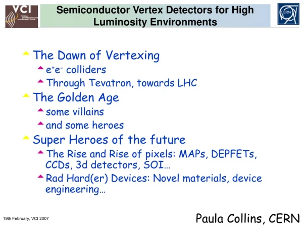
Semiconductor Vertex Detectors for High Luminosity Environments • The Dawn of Vertexing • e+e- colliders • Through Tevatron, towards LHC • The Golden Age • some villains • and some heroes • Super Heroes of the future • The Rise and Rise of pixels: MAPs, DEPFETs, CCDs, 3d detectors, SOI… • Rad Hard(er) Devices: Novel materials, device engineering… Paula Collins, CERN Paula Collins, CERN
Alternatively… To Infinity and Beyond! SLHC Who will be the true superhero of the SLHC era? Paula Collins, CERN
Alternatively…. How do I cope with having 10 quadrillion particles thrown at me?* *1016 fluence / cm2 at 4cm SLHC Paula Collins, CERN
The LEP era Singapore Conference, 1990 ‘The LEP experiments are beginning to reconstruct B mesons… It will be interesting to see whether they will be able to use these events’ Gittleman, Heavy Flavour Review 10 fun packed years later, heavy flavour physics represented 40% of LEP publications Paula Collins, CERN
Reconstructed B-mesons in the DELPHI microvertex detector semiconductor vertex detectors used for vertexing flavour tagging, lifetimes.. help in tracking triggering even dE/dx… used at all current HEP collider experiments exploits great precision and small beampipes and more… B hadron Vertex Primary Vertex Paula Collins, CERN tB 1.6 ps l = ctg 500 mmg
Challenge of the LHC ATLAS at full luminosity L=1034 cm-2 s-1: • ~23 overlapping interactions in each bunch crossing every 25 ns ( = 40 MHz ) • inside tracker acceptance (|h|<2.5) 750 charged tracks per bunch crossing • per year: ~5x10¹⁴ bb; ~1014 tt; ~20,000 higgs; but also ~1016 inelastic collisions – impact parameter resolution important • severe radiation damage to detectors: • Fast Hadron dose at 4 cm after 10 years/500 fb-1 is 3 x 1015 cm-2 • Fast Hadron Dose at 22 cm after 10 years/ 500 fb-1 is 1.5 x 1014 cm-2 • detector requirements: speed, granularity, radiation hardness LHCb neq/cm2 per year Paula Collins, CERN radius [cm]
What of the future? The problems pile up….. Paula Collins, CERN
SLHC environment Phase 1:no major change in LHC L = 2.34 ∙1034cm-2s-1(higher beam current)Phase 2:major changes in LHC L = 4.6 ∙1034cm-2s-1with (BL/2, qc) L = 9.2 ∙1034cm-2s-1 with (fill all bunches) Phase 3:increase beam energy to 14 TeV (9 to 17 T magnets) • Integrated Luminosity 2500 fb-1 = 5 x LHC • dictates technology choice • Peak luminosity 1035 cm-2 s-1 = 10 x LHC • dictates detector granularity • Scenarios dominated by 50ns or 25 ns running • Detector R&D focused on • short term replacement/upgrades e.g. replacement of ATLAS b layer after 2-3 years (1015 neq), CMS Phase 1 pixel replacement, replacement of LHCb VELO … • SLHC upgrades (major changes expected to modules and electronics SLHC fluences R=75cm, 1.5 1014 cm-2 3.5 MRad, charged hadrons 20% R=20cm, 1 1015 cm-2 30 MRad, charged hadrons 50% R=4cm, 1.6 1016 cm-2 400 MRad, charged hadrons 100% Paula Collins, CERN Mika Huhtinen
Point defects + clusters Dominated by clusters Non Ionizing Energy Loss NIEL: displacement damage A common language: “1 MeV neutron equivalent” Use the NIEL scaling factors NIEL allows us to look into the future and predict what will happen in complex environments (!) Is known to fail for neutrons/charged hadrons in some cases Paula Collins, CERN
Effective Doping Changes • negative space charge builds up, depletion voltage changes • Junction moves from p+ to n+ side Depletion voltage [V] Fluence • Annealing effects • Buildup of negative space charge worsening in time • Strongly temperature dependent: 500 years @ -10oC = 21 hours at 60oC! Depletion voltage [V] time [years] Radiation Damage: Traditional Villains • Increased Leakage Current • Noise • Hard to bias • strong temperature dependence – cooling essential e.g. I(-10 oC)=1/16 I(20oC) • anneals with time and temperature DI/V=a * f a, the damage parameter, very consistent for a wide range of impurities and silicon types Paula Collins, CERN
New Villain: trapping Trapping is characterized by an effective trapping time eff for e- and h: where Increase of 1/ with fluence 1/ changes with annealing Huge Decrease in CCE? Paula Collins, CERN
after type inversion Neff=ND-NA<0 - Radiation Damage: Is Neff really so bad? V. Chiochia et.al. IEEE Trans. Nucl. Sci 52 (2005) 1067 Charge collection measured using cluster profiles in a row of pixels illuminated by a 15º beam and no magnetic field F = 6x10¹⁴ n/cm2 Model with constant space charge density does not describe the measured charge collection Paula Collins, CERN
Two trap model EA/D= trap energy level fixed NA/D = trap densities from fit se/h = trapping cross sections from fit F1=6x10¹⁴ n/cm2, NA/ND=0.40, sh/se=0.25 • Data --- Simulation n+-p junction n-p+ junction E Paula Collins, CERN V.Chiochia, Vertex 05
Radiation damage as experienced in running HEP experiments NA60 first use of pixels in high multiplicity experiment dimuon production by 158 gev indium ions 16 planes of silicon pixel detectors 12.8 x 13.6 mm2 active area 32 x 256 cell matrix 50 x 425 um2 cell size ALICE 1LHCb readout chips ATLAS faster pixels radiation damage type inversion after 4 weeks running 4x10¹² ions on target ~1013 neutrons equivalent Paula Collins, CERN
Irradiation at CDF/D0 • 2 fb-1 data collected (goal = 5-8fb-1) • L00 (1.4cm) SVXII (2.5-10.6cm), ISL • Ionising dose measured with TLDs • 3cm z<45cm: 300 +- 60 kRad/fb-1 • scales as 1/ra (1.5 < a < 2.1) • L00 2 MRad, SVX layer 0 800 kRad • Measured depletion voltages both with signal and noise methods Ignacio Redondo, CMS workshop, 20th October 2006 L0 depletion Voltage Paula Collins, CERN
tackling the villains • New Sensor Materials • Silicon Carbide • Amorphous silicon • Compound semiconductors • Diamond • Defect Engineering • Oxygen enriched silicon • Cz silicon • … • Device Engineering • p-type silicon detectors • thin detectors • 3D • Monolithic devices • DEPFETS • MAPS • CCDs with on situ storage • SOI … • Operational conditions • Cryogenic operation See talk of S. Eckert 3D silicon stacks -> see talk of J. Mnich -> see talk of W. Dulinkski -> see talk of Toru Tsuboyama + posters of Bamberger, Traversi, Gabrielli, Servoli, Luuka, Paula Collins, CERN
Reminder: figure shown at VCI 2001 – silicon experts learn about weighting field!! new kid on the block: p-type substrate p side n side ATLAS ATLAS • n-on-n already preferred option for ATLAS, CMS, and LHCb • Faster charge collection • underdepleted operation an option • After type inversion n-on-n effectively becomes p-on-n: Why not start with step p type substrates Efficiency Vbias Vbias NIM A 450 (2000) 297 p side n side LHCb LHCb Resolution [mm] Vbias Vbias Paula Collins, CERN NIM A 440 (2000) 17
S1 S1 S2 S2 S1 S2 p type continued • RD50 collaboration with CNM, Micron • FZ, DOFZ, MCz silicon • pads, strips, pixels • p-stop, p-spray • Many groups: Liverpool, IFIC, KEK, INFN.. • Advantages of p-type • high field region always on the strip side – no need for (expensive) double sided processing • easier handling • proven radiation hardness • collect electrons – slightly less susceptible to trapping after neutron irradiation • indication of good annealing behaviour (as measured with CCE) cooling, handling • Effort going into characterising strip isolation methods (as for n-in-n) p-stop p-spray/p-stop p-spray high-field region depends on Qox high-field regions high-field regions compromise Cint, VBR improve with radiation (Oox), worse initially Cint, VBR degrade with radiation (Oox), better initially Paula Collins, CERN
0.7x10¹⁵ 1.9x10¹⁵ 4.7x10¹⁵ 10x1015 M Lozano, this conference p type; irradiation of short strip devices Detector geometry: Thickness=300 mm, strip pitch=80 mm, implant width= 18 mm, LHC speed readout (SCT128A-HC), beta source measurements n-in-p : standard FZ • ~40% charge loss after 3x10¹⁵ p/cm2 (23 GeV) • ~7000 e after 7.5x10¹⁵ p/cm2 (23 GeV) n-in-p : annealing • 3 x 10¹⁵ n/cm2 • Vdep ~ 1200 V Vfd Vfd~1200 V Vfd>2500 V G. Casse, this conference P.P. Allport et al., IEEE Trans. NS 52(5) (2005) 1903. Annealing behaviour w.r.t. CCE spectacular Performance superior to p-on-n (n-on-n unknown at these fluences) Paula Collins, CERN
p type continued • Full scale sensors manufactured for LHCb and placed in final detector layout in test beam • 8.4 cm diameter sensors • strip pitch 40-100 mm • excellent leakage currents • fraction of bad strips < 1% • preliminary results show pre-irradiation performance very comparable to n-in-n – technology feasibility demonstrated T. Bowcock Paula Collins, CERN
Oxygen lessons from LHC Based on RD48 discovery that Vfd varies more slowly for oxygenated sensors, DOFZ chosen for detectors in most irradiated regions of ATLAS,CMS,LHCb However, note that neutron irradiation is 3xmore damaging and constant for all materials… try materials naturally rich in Oxygen • Czochralski silicon • Pull Si-crystal from a Si-melt contained in a silica crucible while rotating. • Silica crucible is dissolving oxygen into the melt high concentration of O in CZ • Material used by IC industry (cheap), now available in high purity for use as particle detector (MCz) • Epitaxial silicon • Chemical-Vapor Deposition (CVD) of Silicon • CZ silicon substrate used diffusion of oxygen • Growth rate about 1mm/min • Excellent homogeneity of resistivity • 150 mm thick layers produced (thicker is possible) • price depending on thickness of epi-layer but not extending ~ 3 x price of FZ wafer Paula Collins, CERN
EPIlayer CZ substrate Oxygen concentration in FZ, Cz, and EPI Epitaxial silicon Cz: high homogeneous concentration and formation of Thermal Donors (reducing acceptors due to radiation) [G.Lindström et al.,10th European Symposium on Semiconductor Detectors, 12-16 June 2005] • EPI: inhomogeneous O concentration due to diffusion from substrate into epi-layer during production • DOFZ: inhomogeneous oxygen distribution, increasing with time at high temperature Paula Collins, CERN
MCz-n Helsinki MCz silicon irradiation with charged hadrons FZ • Gradient of slope after minimum (b) is smaller for MCz than for FZ for 10 MeV, 50 MeV and 24 GeV proton irradiation • The effective trap introduction rate for both electrons and holes is similar for MCz, FZ, and DOFZ silicon • Leakage current behaviour is also similar DOFZ Cz G. Pellegrini et. al “Annealing Studies of magnetic Czochralski silicon radiation detectors” E. Tuovinen et. al. 4th RD50 workshop Annealing behaviour Many groups studying Cz, MCz: INFN, Glasgow, BNL, HIP, Purdue, Liverpool, Rochester… Paula Collins, CERN
MCz TCT measurements 5x10¹⁴ p/cm2 • TCT measurements confirm that after irradiation with charged hadrons the material does not type invert • the trap introduction rate for holes and electrons is similar for FZ, DOFZ and MCz silicon • This behaviour can be understood qualitatively as a build up of donors, which overcompensates the (classical) introduction of acceptors electron collection hole collection High field High field Low field Low field Paula Collins, CERN Time [ns] 14 A. Bates, VERTEX 04
n+ p+ E2 E1 hn Eb 2 1 W2 W1 Wb B MCz TCT measurements continued F 1 MeV, = 5 ×1014 cm-2 CZ n-Si, [D. Menichelli, RD50 Workshop, Nov..2005] p+ • Irradiation with neutrons shows a more complex picture • High field region on n+ side implies type inversion • In this respect MCz and FZ behave similarly n+ Φ (1014n*cm-2) E(x) is non-uniform in these sensors (as in other, non MCz, heavily irradiated structures) Consider 3 regions: Neff>0, electrically neutral, Neff<0 reverse current flow induces electric field in electrically neutral base For detector performance, Vdep is an “abstract concept” More important to consider CCE, charge collection time etc. Paula Collins, CERN Verbitskya et.al. NIM A 557 (2006) 528
MCz CCE m bruzzi et al, hiroshima symposium 2006 p-on-n MCz microstrip device, 200 ns shaping time proton irradiated 90% CCE achieved at 500V for 3.3 x 10¹⁴ neq p type MCz Si diodes, proton irradiated AC coupled r/o shaping time 2.4us At overdepletion 90% CCE for 6.8 x 10¹⁴ neq Sadrozinski STD07 Simulation predicts for 300 and 200 um thick a S/N of 10 at 3 x 10¹⁵ which would be adequate for operation of a detector Paula Collins, CERN
EPI silicon G. Lindström et al. neutron irradiation G. Kramberger et al., 8th RD50 workshop SMART coll., 8th RD50 workshop Kramberger et al 8th RD50 workshop June 2006 Neutron irradiation: excellent peformance of Neff evolution; no SCSI for 50 mm sample CCE measured with mips : 3200 electrons after 8 x 10¹⁴ neq / cm2 Superrad hard : Fledermaus-man? (performs best in superhero mode…) Paula Collins, CERN
With cooling when not operated Without cooling when not operated EPI silicon : annealing behaviour Kramberger et al 8th RD50 workshop June 2006 • Annealing behaviour shows drop of Vdep in time Using the LHC operation model: • Radiation @ 4cm: eq(year) = 3.5 1015 cm-2 • SLHC-scenario: • 1 year = 100 days beam (-7C) • 30 days maintenance (20C) • 235 days no beam (-7C or 20C) • Operation without cooling is beneficial!!! G.Lindström et al.,10th European Symposium on Semiconductor Detectors, 12-16 June 2005 (Damage projection: M.Moll) Paula Collins, CERN
Grain size: ~100-150μm growth substrate Diamond Polycrystalline Diamonds traditionally grown by CVD • large band gap and strong atomic bonds give fantastic radiation hardness • low leakage current and low capacitance both give low noise • 3 (1.5) times better mobility and 2x better saturation velocity give fast signal collection • Ionization energy is high: MIP 2x less signal for same X0 (w.r.t. SI) • Diamond: 13.9ke- in 361 m • SI: 26.800 ke- in 282 m • In Polycrystalline Diamond grain-boundaries, dislocations, and defects: • limits carrier lifetime, mobility and charge collection distance and position resolution • Diamond as detector material now well established with BCM as first large scale (HEP) application • Detector application (pixel, strip, pad) demonstrated Paula Collins, CERN
Radiation Hardness of pCVD diamond • pCVD charge collection distances of 250-300 mm now routinely achieved • charge collection distance saturates at 1V/mm • pCVD detectors have been built as pixel,pad, strip detectors • Proton irradiation of strip detectors to 2.2x10¹⁵/cm2: • 15% loss of S/N at 2.2x10¹⁵/cm2 • Decrease of leakage current (~ pA) • Improvement of resolution by ~35% - irradiated material is more “uniform” • Proton irradiation to 1.8 x 10¹⁶/cm2 • 75% loss of signal • S/N performance > 10 Paula Collins, CERN
Single Crystal Diamond • Single crystal diamond has been fabricated with Element six ≈ 10 mm × 10mm, >1 mm thickness. • Largest scCVD diamond ≈ 14 mm × 14 mm. Most probable charge versus thickness • High quality scCVD diamond can collect full charge at 0.2 V/um • Width of Landau distribution is ≈ 1/2 that of silicon, ≈ 1/3 that of pCVD diamond • radiation hardness under study d=320 μm QMP=9500e- • Excellent mobility. For this sample: • µ0h = 1714 cm2/Vs, µ0e = 2064 cm2/Vs High drift velocity better lifetimes charge trapping might not be an issue Paula Collins, CERN
Irradiation: 3d detectors Proposed by Parker, Kenney 1995 3D Device Planar Device • Maximum drift and depletion distance governed by electrode spacing • Lower depletion voltages • Radiation hardness • Fast response • same technology: dope edges of sensor for edgeless detection efficiency • At the price of more complex processing • Narrow dead regions at wells Unit cell defined by e.g. hexagonal array of electrodes Paula Collins, CERN
p n p n (not like this) How do we make the holes? Paula Collins, CERN
3d detector processing d D Non Standard Processing: Wafer bonding, Deep reactive ion etching , Low pressure chemical vapor deposition, Metal deposition Mass production expensive 2) FILLING THE ELECTRODES 1) ETCHING THE ELECTRODES Aspect ratio: D:d = 11:1 IR picture of 2 bonded wafers LOW PRESSURE CHEMICAL VAPOR DEPOSITION (Electrodes filling with conformal doped polysilicon) 2P2O5 +5 Si-> 4P + 5 SiO2 2B2O3 +3Si -> 4 B +3 SiO2 WAFER BONDING (mechanical stability) Si-OH + HO-Si -> Si-O-Si + H2O DEEP REACTIVE ION ETCHING (electrodes definition) Bosh process SiF4 (gas) +C4F8 (teflon) METAL DEPOSITION Shorting electrodes of the same type with Al for strip electronics readout or deposit metal for bump-bonding 290mm C shaped test structure ~1 mm difference between top and bottom Paula Collins, CERN
3d detectors: characteristics Efficiency measured in testbeam 98% rise time seen on oscilloscope Aug 2006, H8 CERN beam line 100 GeV/c pions 4000 e threshold 40V depletion Institutes: Stanford Brunel/Manchester Hawaii/LBL New Mexico Glasgow Freiburg Bonn Praha Genova Oslo +++ Paula Collins, CERN v
electrode spacing 71 mm n type before irradiation Irradiated with reactor neutrons signal height measured on scope 3d detectors: radiation hardness Compilation plot from C. da Via M Lozano, n-on-p this conference EPI Paula Collins, CERN
Different Geometry: 3D devices 1um Passivation Metal 0.4um Oxide • Design proposed by RD50 collaboration (IRST, CNM, Glasgow) • much simplified process – no need for support wafer during production • single sided processing with additional step of etching and B diffusion 5mm P-stop p+ 50mm n+ doped 10mm TEOS 2um 300mm Poly 3mm p- type substrate p+ doped p+ doped 50mm Oxide See S. Eckert talk for beautiful results Metal 55um pitch Paula Collins, CERN
t t event at 350 GeV What about the ILC? At LC: “x sections are tiny” “No radiation issues” “Triggerless operation possible” “Modest rates” Why not use a LEP detector? we need to trim the X0! LC physics demands Excellent Vertexing (b,c,t) and Tracking a in a high B field a with energy flow Paula Collins, CERN
Silicon for vertexing @ the ILC Required Vertexing performance Flavour tagging: beauty + charm Vertex detector characteristics point resolution 1-5 mm Thickness ~ 0.1 % X0 5 layers Inner radius ~ 1.5 cm radiation tolerance ~ 360 kRad / year discriminate b from background • Use a silicon based pixel detector • Confine the background with a big solenoidal field discriminate b from c disentangle complex events h 12 jets background: mainly e+/e- pair production due to beamstrahlung d (IP) < 5 mm 10 mm/(p sin3/2q) (best SLD 8 mm 33 mm/(p sin3/2q)) [C.Büssser, DESY] Paula Collins, CERN
Train/rf pulse Timing @ the ILC Time a at ILC, keep occupancy reasonable by reading out innermost layer in 50 msec Paula Collins, CERN
Silicon Trends Basic idea amplifier • Start with high resistivity silicon • More elaborate ideas: • n+ side strips – 2d readout • Integrate routing lines on detector • Floating strips for precision • Stripixels: 2d readout Al strip p+ + + SiO2/Si3N4 - - + n bulk + n+ - + Vbias Hybrid Pixel sensors Chip (low resistivity silicon) bump bonded to sensor Floating pixels for precision chip chip n+ p chip n+ DEPFET: Fully depleted sensor with integrated preamp chip MAPS: standard CMOS wafer Integrates all functions CCD: charge collected in thin layer and transferred through silicon Paula Collins, CERN
15 V 0V 0V + + + DEPFET sensors Kemmer, Lutz, 1987 R&D for tracking ~ 2000 + • Amplifying transistor integrated into high resistivity silicon detector • Low noise operation possible at room temperature • Thinning possible to 50 mm Image of DEPFET team R&D: pixel size, power, thinning, speed, radiation tolerance 2005: 128x64 36mmx29mm prototypes 512 x 512, and 128 x 2048 array under development Paula Collins, CERN
Testbeam setup: 5 DEPFET planes Switcher chip provides gate voltages PCB ‘hybrid’ with DEPFET matrix, 2 x SWITCHER, 1 x CURO DEPFET Matrix 64x128 pixels 36 x 28.5µm2 ~ row clear Switcher chip provides clear voltages Sources row gate double pixel Sources Drain 1 Drain 2 Sources Paula Collins, CERN double metal matrix
Ionising dose to ~1MRad without degradation in performance of pixel HV switcher does not survive this dose New switcher layout with rad hard technology and “stacked transistors” submitted and will be tested soon DEPFET • S/N for 450 mm thick sensor 110 • upper limit on position resolution ~8 mm (contains an estimated 7 um contribution from low energy tracks – data from CERN testbeam will improve this) • cluster sizes for inclined tracks comparable to simulation FE 55 spectrum from irradiated pixel measured at room temperature noise of 3.5 e (was 1.6 before irradiation) Paula Collins, CERN P Fisher et. al. Vertex 06
sensor wafer handle wafer 2. bond wafers with SiO2 in between 3. thin sensor side to desired thickness. 4. process DEPFETs on top side 5. etch backside up to oxide/implant 1. implant backside on sensor wafer Thinning active DEPFET area (~ 50µm thick) Estimated material budget for first layer 0.11% X0: pixels, 50 mm thick, 0.05% X0 chips, 50 mm thick, 0.008% X0 perforated frame, 300 mm thick, 0.05% X0 CUROReadout chips leakage current Thinned diode structures: leakage current: < 1 nA/cm2 SWITCHERSteering chips Possible ILC implementation 100pA / cm2 Paula Collins, CERN
Monolithic Active Pixel Sensors (MAPS) 1999 – R&D on CMOS MAPS 1999 – small scale prototypes 1999-2000 first beam tests 2001 – large prototypes 2005 – dedicated application specific chips • Same unique substrate for detector and electronics • No connections(e.g. bumps) • Radiation hardness (no bulk charge transfer) • Advantages of CMOS process: Easy Design/good yield/low power/Rad hard • Very small pixel sizes achieveable Mimosa I …….. IV V ……. VIII …….. IX …… X …….. XIV .. Process 0.6 mm AMS0.35 mm AMS0.6 mm AMS0.25 TSMC 0.35 mm AMS 0.25 mm TSMC 0.35 mmAMS Epi layer 14 mm 0 (!!!) 14 mm 8 mm 14 mm 8 mm 0 # pixels 64x64x4 64x64x4 1Mx7 7k 7k 16k 16k Paula Collins, CERN
Signal to Noise Resolution [mm] MIMOSA V MIMOSA I MAPS Beam Test Results MIMOSA I MIMOSA II MIMOSA V Resolution 1.4 mm 2.2 mm 1.7 mm Efficiency at S/N > 5 99.5 % 98.5 % 99.3% Two track separation 30 mm thinning possible to 50 mm R&D for high temperature operation (STAR upgrade) Paula Collins, CERN
MAPS: Radiation Hardness Expectations at ILC (for 3 years of nominal running): • “non-ionizing” radiation: 3.1010 neq/cm2 • MIMOSA I, II, V irradiated with 1013 n/cm2 • Gain -> constant • Noise -> constant • Leakage current a moderate rise • collected charge a 50-70% of initial value (smooth decrease after 1012 or few x 1011 ) MIMOSA9chip irradiated with 1011n/cm2 • test beam: S/N ~ 25, e > 99.9% • dose increased to 1012n/cm2 with good results - “ionizing” radiation: 5.4.1012e(10MeV)/cm2 MIMOSA5 and MIMOSA9chips irradiated at Darmstadt with 1013e(9.4MeV)/cm2 • test beam (MIMOSA9): S/N ~ 23, e > 99% - slight deterioration but still excellent performance michael deveaux Paula Collins, CERN
Charged Coupled Devices - CCDs CCDs invented in 1970 – widely used in cameras, telescopes etc. Tracking applications for HEP: 1980-1985 NA32 120 kpixels 1992-1995 SLD 120 Mpixels 1996-1998 SLD upgrade 307 Mpixels ILC 799 Mpixels ~1000 signal electrons are collected by a combination of drift and diffusion over a ~20mm region just below surface 10V 2V • Small pixel size – 20 x 20 mm • Possibility of very thin detectors • Column parallel readout: serial register -> direct bump bonding to chip Paula Collins, CERN
Layer Radius (mm) CCD lxw (mm x mm) CCD Size (Mpix) Clock / readout time Background (Hits/mm2) Integrated background (kHits/train) 1 15 100 x 13 3.3 50 MHz/50 ms 4.3 761 5 60 125 x 22 6.9 25 MHz/250 ms 0.1 28 CCD R&D for ILC requirements • Speed up readout • 5 MHz readout -> 50 MHz • Reduce clock amplitudes 10V->2V • Build with high resistivity epitaxial material • distributed busline over entire image area • Study radiation resistance to LC doses of 100Krad ionising radiation + 5 x 10⁹ neutrons • Temperature dependence CCD 55Fe spectrum: 1MHz 2V clocks noise ~ 60 e- Paula Collins, CERN