Download
1 / 13
130 likes | 241 Vues
This report outlines the progress of the PHENIX pilot chip, focused on the development and testing of a new digital ASIC. It highlights the functionality and test results of the chip, including its integration with optical data links and control signals. The document details the testing setup, the packaging of chips from CERN, and the outcomes of initial functionality tests. Furthermore, it discusses the GOL test setup utilizing high-speed deserializer evaluations, providing insights into the serialization and comparison methodologies used in testing.

E N D
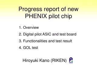
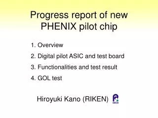
Progress report of new PHENIX pilot chip 1. Overview 2. Digital pilot ASIC and test board 3. Functionalities and test result 4. GOL test Hiroyuki Kano (RIKEN)
Pilot Module Overview 4x32bit@10MHz data Digital pilot ASIC Optical data link GOL Pilot module (on-detector) DAQ (counting room) CLK Sensor Readout chip Command Readout chip control signals 4x BUS
OE/EO OE/EO OE/EO OE/EO OE/EO OE/EO OE/EO Digital pilot Digital pilot Digital pilot Digital pilot Digital pilot Digital pilot Digital pilot Why New Digital pilot ASIC? B. For PHENIX 4x bus A. ALICE original data data data data G G 32b 32b CLK A ctrl ctrl data G 32b C.PHENIX pilot w/ new chip ctrl data data G G 2x32b 32b New chip ctrl ctrl data data G G 2x32b 32b CLK A ctrl CLK A ctrl 1.6Gbpsmode bus opt bus opt = Analog monitor chip G A G G = Gigabit Optical Link (GOL)
Digital pilot ASIC, Packaging, and Test board Bare-chips were delivered from CERN(IBM). [11 Oct.] Bare-chips ware packaged for the test purpose by Fujitsu. (QFP256, 23packages) [19 Oct.] ASIC test board with chip was delivered. [22 Nov.] Packaged ASIC Bare chip Digital pilot ASCI test board 28mm 6mm QFP256 package 8mm
PHENIX Pilot Chip Overview Test pattern generating Pilot Chip has three main blocks 1.Multiplexer converts readout data; 4x32bit@10MHz to 1x32bit@40MHz. 2.Readout chip controller make readout sequence. 3.Command decoder decodes commands from serial stream. Test setup for the new digital pilot ASIC Probing Test board Pixel data input (10MHz) 32bit bus width DATA_0 MUX DATA_1 pixel data output (40MHz) FO Feedback strobe Readout-chip control Readout chip Controller nevr CE Shreg clev Serial control stream L1 L2y L2n rst Command Decoder JTAG JTAG(GOL) JTAG(RO)
Command Decoder Below 2 pictures shows you that command signal corresponding to serial stream is probed. in Commands, JTAG, etc Serial control stream Command decoder serial stream in out reset_gol GOL reset command by new chip [1-DEC-04] serial stream in testpulse out testpulse command by new chip [1-DEC-04]
Readout chip Controller This picture shows the readout sequence; The nevr_i and ce_n are generated from L1 and L2. Readout sequence by new chip [1-DEC-04] nevr_i ce_0 Wave form of readout sequence (ALICE digital pilot document) ce_1 Reference :http://a.home.cern.ch/a/akluge/www/work/alice/spd/spd_documents/ops2003book.pdf ce_9
MUX CLK40 and output data by new chip [9-DEC-04] slot0 slot1 slot2 slot3 slot0 slot1 slot2 slot3 ….. This test pattern is; BUS A31-0 pattern = up counter; 00000000,11111111,22222222,… BUS B31-0 pattern = down counter; FFFFFFFF,EEEEEEEE,DDDDDDDD,… This picture shows that the original data bus (BUS A31-0) and additional data bus (BUS B31-0) can be processed correctly. Test pattern generating Probing Test board Reference :http://a.home.cern.ch/a/akluge/www/work/alice/spd/spd_documents/ops2003book.pdf
Summary of ASIC test • Packaging and test board assembly are finished. • Result of functionality test seems fine, but not completed yet. • Functionality test will be finished in this month.
GOL test setup Vertex2pro GOL Vertex2-pro evaluation board: =Vertex2-pro interface board Vertex2-pro has integrated hi-speed deserializer. Optical fiver EO converter GOL test board: It can be mounted on Vertex2-pro board via PMC connector GOL test full setup OE/EO converter: Agilent evaluation board
FPGA program overview • GOL test program is based on the xilinx evaluation source. • Vertex2-pro generates test vector, serializes, and comparisons between generated vector and GOL output vector. serialize (integrated) generating test signal comparison deserializer (GOL) display (LED&LCD) Vertex2-pro program
1. 3Gbps→1.6Gbps (cupper wire) Test step RocketIO V2P Vertex2pro • Cupper wire setup [26 Oct.] System test, Developing GB-ethernet protocol, Changing the link speed* • Optical fiver setup [12 Nov.] Optical component test • GOL test TED Vertex2-pro test Board 1.6Gbps (optical fiver) 2. V2P Agilent OE board Agilent EO board 1.6Gbps (optical fiver) *Changing the link speed Vertex2-pro test board has 156MHz crystal for the V2-pro maximum speed. In our case, we need 1.6Gbps. 3. V2P GOL test board Agilent OE board
Summary of GOL test • Test setup is ready now. • Gigabit Ethernet protocol for GOL is developed.