HOMEWORK 4-1
HOMEWORK 4-1. Compute the low and high noise margins using the following transfer curve of a Pseudo-pMOS inverter. HOMEWORK 4-2. The circuits below show different implementations of an inverter whose output is connected to a capacitor.

HOMEWORK 4-1
E N D
Presentation Transcript
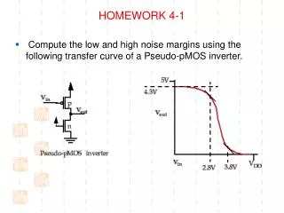
HOMEWORK 4-1 • Compute the low and high noise margins using the following transfer curve of a Pseudo-pMOS inverter.
HOMEWORK 4-2 • The circuits below show different implementations of an inverter whose output is connected to a capacitor. a. Which one of the circuits consumes static power when the input is high? b. Which one of the above circuits consumes static power when the input is low? c. VOH of which circuit(s) is 1.2V? d. VOL of which circuit(s) is 0V? e. The proper functionality of which circuit(s) depends on the size of devices.
HOMEWORK 4-3 • 图示是一种新的逻辑类型—伪PMOS,采用NMOS器件作负载,PMOS器件作驱动。与伪NMOS结构相比,伪PMOS结构的优缺点分别是什么?
HOMEWORK 4-4 Calculate VOL, VOH,VIL,VIH,NML and NMH for a two-input NOR gate fabricated with CMOS technology. (W/L)p= 4 (W/L)n= 1 VT,n=0.7V VT,p=-0.7V μnCox=40uA/V2 μpCox=20uA/V2 VDD=5V
HOMEWORK 4-5 • Consider a straight Metal 2 wire in 180 nm process with the following parameters: the wire length is LW = 5 mm, the wire width is WW = 0.32 μm, sheet resistance for Metal 2 is RS = 0.05Ω, and wire capacitance per one micrometer is cw = 0.2 fF/μm. • Calculate total wire resistance RW and total wire capacitance CW?
HOMEWORK 4-6 Design a resistive-load inverter with R=1KΩ, such that VOL=0.6V. The enhancement-type NMOS driver transistor has the following parameters: VDD=5.0V VT0=1.0V γ=0.2V1/2 λ=0 unCox=22.0uA/V2 • Determine the required aspect ratio, W/L. • Determine VIL and VIH. • Determine noise margins NML and NMH.
HOMEWORK 4-7 Consider a CMOS inverter with the folloeing parameters: nMOS VT0=0.6V unCox=60uA/V2 W/L=8 pMOS VT0=-0.7V upCox=25uA/V2 W/L=12 Calculate the noise margins and the switching threshold VTh of this circuit. The power supply voltage is VDD=3.3V.
HOMEWORK 4-8 Design a CMOS inverter circuit: Use the device parameters as folloe: nMOS VT0=0.6V unCox=60uA/V2 pMOS VT0=-0.7V upCox=25uA/V2 The power supply voltage is VDD=3.3V. The channel length of both transistors is Ln=Lp=0.8um. • Determine the (Wn/Wp) ratio so that the switching threshold voltage of the circuit is VTh=1.4V. • The CMOS fabrication process used to manufacture this inverter allows a variation of the VT0,n value by ±15% around its nominal value. And a variation of the VT0,p value by ±20% around its nominal value. Assuming that all other parameters always retain their nominal values, find the upper and lower limits of the switching threshold voltage VTh of this circuit.
HOMEWORK 4-9 • Use the process parameters obtained in 0.5 μm CMOS process(λ=0.25μm)as follow: For the conductor shown in the figure, calculate the capacitance of the conductor, a. while the conductor area is in metal 1. b. while the conductor area is in polysilicon. c. while the conductor area is in n-diffusion layer.
HOMEWORK 4-10 • Use the same process parameters as 4-8. For the layout shown in the figure, calculate the capacitance of the conductor of the transistor gate.
HOMEWORK 4-11 一个CMOS反相器电路具有以下特性: Cout=100 fF tdr=123.75 ps Cout=115 fF tdr=138.60 ps 反相器是对称设计,kn=kp,VTn=│VTp│。 • 求MOS电阻Rn=Rp和反相器的内部电容CFET。 • 如果两个MOS管的宽度增加为原来的3.2倍,计算Cout=140fF时的延时tdr=tdf=?
HOMEWORK 4-12 • Find the ratio Wp/Wn for transistors in the 3-input NOR gate such that circuit has approximately equal worst-case rise and fall times. Assume the n-type transistors have the same Wn and Ln, that the p-type transistors have the same Wp and Lp, and that effective resistance value for minimum size transistors is Rpmin = 14kΩ and Rnmin = 3.9kΩ. Find the p-type channel width in multiplies of l, if we assume that n-type transistors have minimal width.
HOMEWORK 4-13 What is the primary reason for the reduction in the rise time at the output of the following circuit configurations ? Explain this classic CMOS trade-off (in one sentance).
HOMEWORK 4-14 • Given the n-tree for the function F = A (B+C+D ) , which point (1 or 2) would you connect to GND in order to obtain the fastest fall time, if input A was last arriving signal ? Briefly explain in words. x
HOMEWORK 4-15 Consider the circuit of the following figure. a. What is the logic function implemented by the CMOS transistor network? Size the NMOS and PMOS devices so that the output resistance is the same as that of an inverter with an NMOS W/L = 4 and PMOS W/L = 8. b. What are the input patterns that give the worst case tpHLand tpLH. State clearly what are the initial input patterns and which input(s) has to make a transition in order to achieve this maximum propagation delay. Consider the effect of the capacitances at the internal nodes.
HOMEWORK 4-16 a. Do this two circuits implement the same logic function? If yes, what is that logic function? If no, give Boolean expressions for both circuits. b. Will these two circuits’ output resistances always be equal to each other? c. Will these two circuits’ rise and fall times always be equal to each other? Why or why not?

